TIDT179A may 2020 – april 2023
3.1 Switch Node
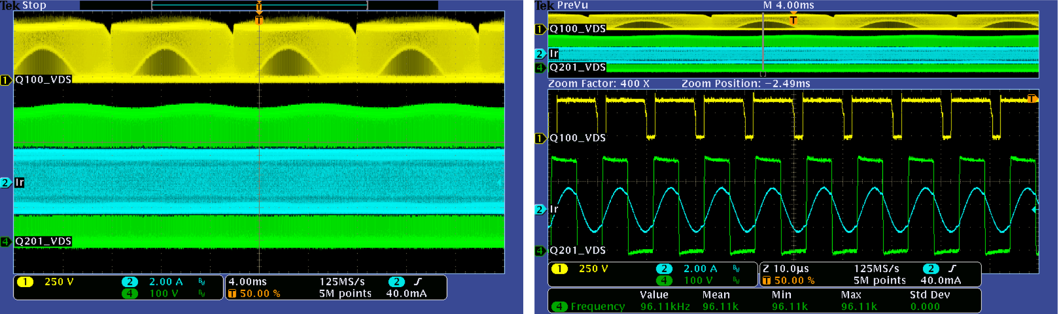
The photo below shows the switch node voltage (Q100 & Q201 Vds) and resonant current waveforms at full load. The input voltage is 230Vac and outputs full load. (CH1: Q100_Vds, CH2: Q201_Vds, CH4: resonant current)
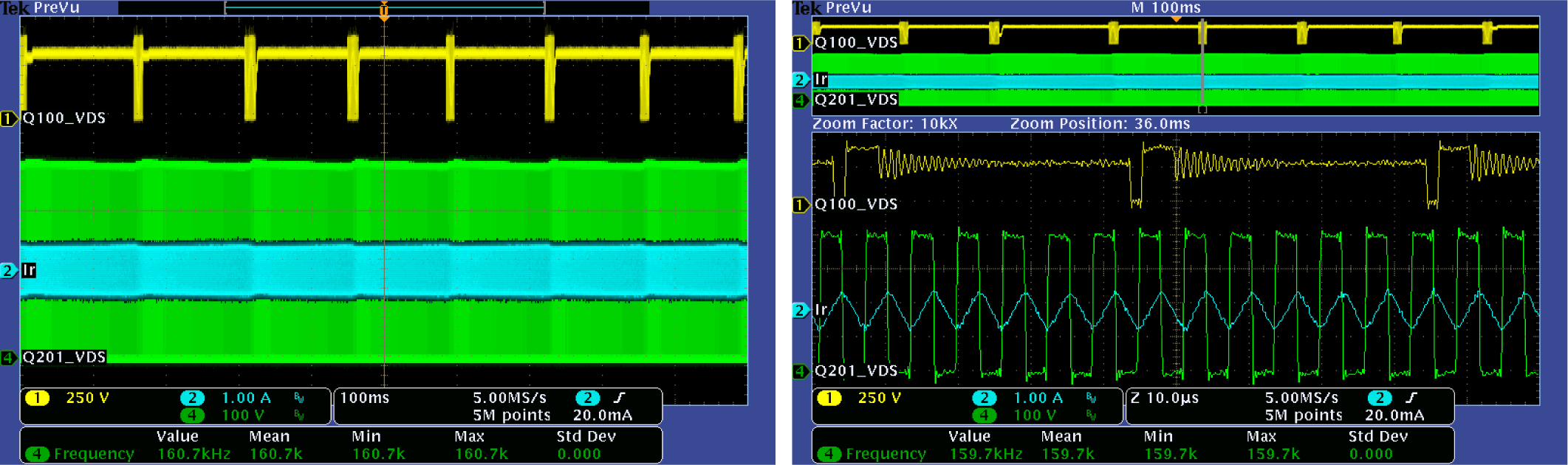
The photo below shows the switch node voltage (Q100 & Q201 Vds) and resonant current waveforms at no load. The input voltage is 230Vac and outputs no load. (CH1: Q100_Vds, CH2: Q201_Vds, CH4: resonant current)
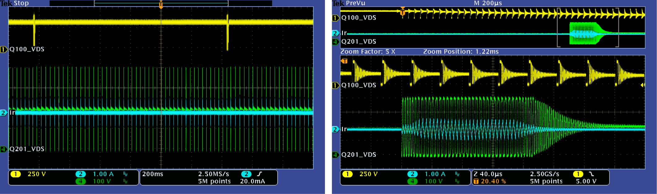
The photo below shows the switch node voltage (Q100 & Q201 Vds) and resonant current waveforms at standby. The input voltage is 230Vac and outputs no load. (CH1: Q100_Vds, CH2: Q201_Vds, CH4: resonant current)
The photo below shows the input voltage and input current of PFC stage at 115Vac/60Hz and full load conditions (CH1: Input Voltage; CH2: Input Current)
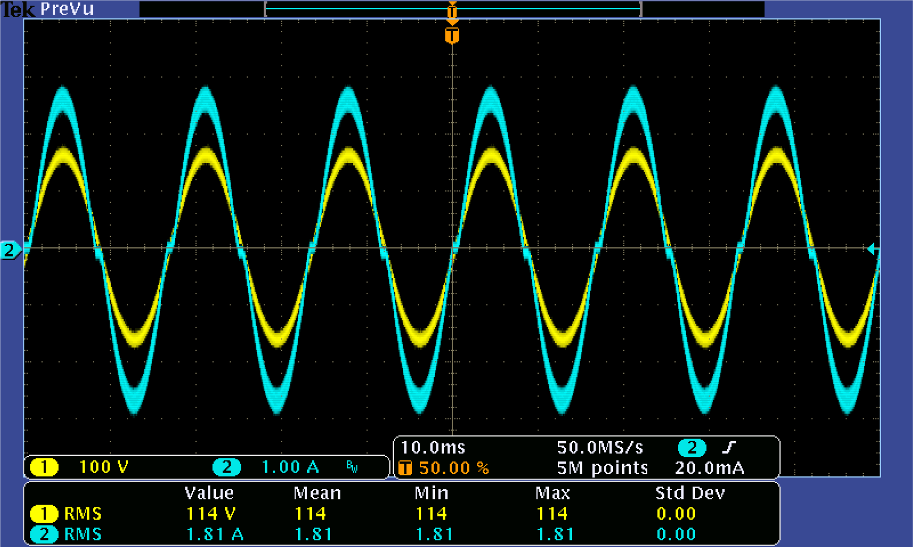
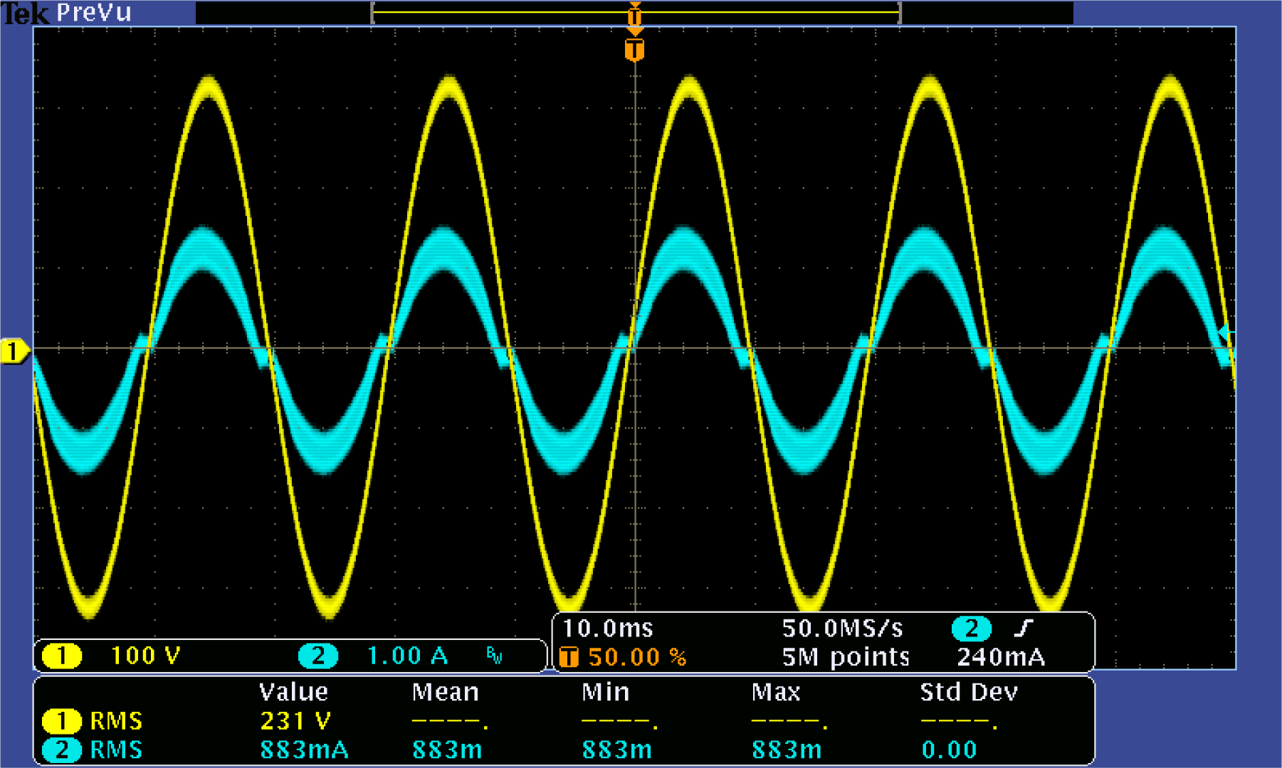
The photo below shows the input voltage and input current of PFC stage at 230Vac/50Hz and full load conditions (CH1: Input voltage; CH2: Input current)