TIDT289 July   2022


  1.   Description
  2.   Features
  3.   Applications
  4. 1Test Prerequisites
    1. 1.1 Voltage and Current Requirements
    2. 1.2 Considerations
    3. 1.3 Dimensions
  5. 2Testing and Results
    1. 2.1 Efficiency Graphs
    2. 2.2 Load Regulation
      1. 2.2.1 Output Voltage 1 (1.1 V)
      2. 2.2.2 Output Voltage 2 (3.3 V)
    3. 2.3 Thermal Images
    4. 2.4 Bode Plots
      1. 2.4.1 Output Voltage 1 (1.1 V at 6 A)
      2. 2.4.2 Output Voltage 2 (3.3 V at 1 A)
  6. 3Waveforms
    1. 3.1 Switching
      1. 3.1.1 Output Voltage 1 (1.1 V at 6 A)
        1. 3.1.1.1 Test Point TP3may be TP3 can be linked to the schematic which will be uploaded with the design (Pin SW_B0)
        2. 3.1.1.2 Test Point TP9may be TP9 can be linked to the schematic which will be uploaded with the design (Pin SW_B1)
      2. 3.1.2 Output Voltage 2 (3.3 V at 1 A)
    2. 3.2 Output Voltage Ripple
      1. 3.2.1 VOUT1 (1.1 VD at 6 A) and VOUT2 (3.3 V at 1 A)
      2. 3.2.2 VOUT3 (2.5 V at 0.3 A) and VOUT4 (1.1 V at 0.4 A)
    3. 3.3 Input Voltage Ripple
    4. 3.4 Load Transients
      1. 3.4.1 Switching Load on Output Voltage 1 (1.1 VD)
        1. 3.4.1.1 Output Voltage 1 (VOUT1)
        2. 3.4.1.2 Cross Talking on VOUT2 (3.3 V)
      2. 3.4.2 Switching Load on Output Voltage 2 (3.3 V)
    5. 3.5 Start-Up Sequence
      1. 3.5.1 Hot Plug-In
      2. 3.5.2 Enable with Switch S1
        1. 3.5.2.1 All Traces
        2. 3.5.2.2 Without VOUT1
        3. 3.5.2.3 Without VOUT4
    6. 3.6 Shutdown Sequence
      1. 3.6.1 Hot Plug Off
      2. 3.6.2 Disable With Switch S1
        1. 3.6.2.1 All Traces
        2. 3.6.2.2 Without VOUT1
        3. 3.6.2.3 Without VOUT4

All Traces

GUID-20220609-SS0I-DCHX-9BV2-LLVZKDS0VSSN-low.jpg

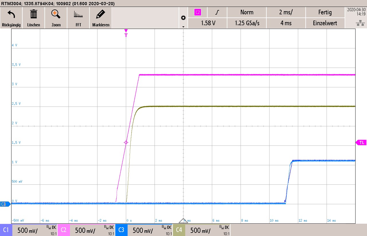
Ch1

VOUT1 (1.1 V at 2 A )

500 mV / div


Ch2

VOUT2 (3.3 V at 0.1 A)

500 mV / div


Ch3

VOUT4 (1.1 V at 0.4 A)

500 mV / div


Ch4

VOUT3 (2.5 V at 0.3 A)

500 mV / div


2 ms / div

20-MHz bandwidth

Figure 3-12 Enable With Switch S1; 3.3 VOUT, 2.5 VOUT, Then After 11 ms Both are 1.1 VOUT
Note:

Both 1.1 VOUT traces have almost identical shape. In Section 3.5.2.3 and Section 3.5.2.2 these traces are displayed separately.