TIDT298 July   2022


  1.   Description
  2.   Features
  3.   Applications
  4. 1Design Information
    1. 1.1 Voltage and Current Specifications
    2. 1.2 Dimensions
    3. 1.3 System Schematic
  5. 2Testing and Results
    1. 2.1 Output Voltage Regulation
    2. 2.2 Efficiency Graphs
    3. 2.3 Efficiency Data
    4. 2.4 Thermal Images
  6. 3Waveforms
    1. 3.1 Switching
    2. 3.2 Output Voltage Ripple

Switching

The following waveform is the switch node at 12-V input, and 100 mA on both HS and LS rails.
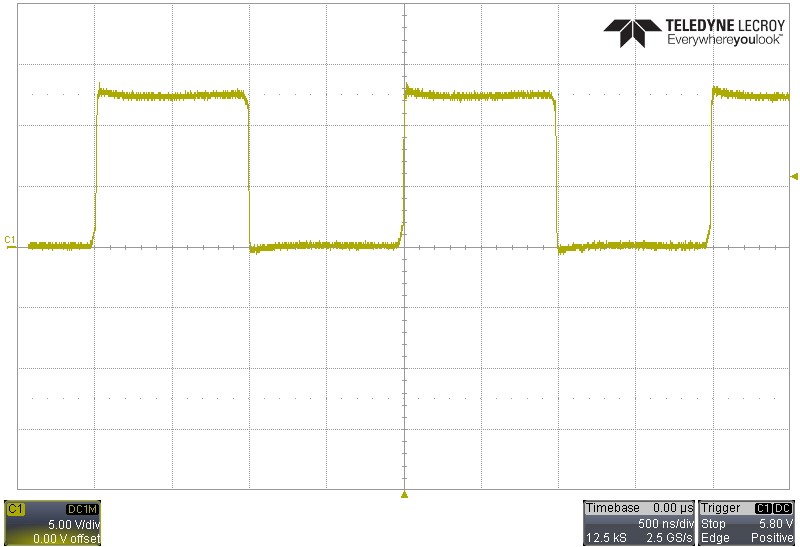
GUID-20220630-SS0I-TFCF-71SR-CTGVRJJ9HJRX-low.jpg Figure 3-1 Switch Node: 12-V Input, 100 mA on Both HS and LS Rails