TIDT333 may 2023
2.4 Bode Plots
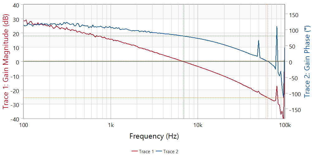
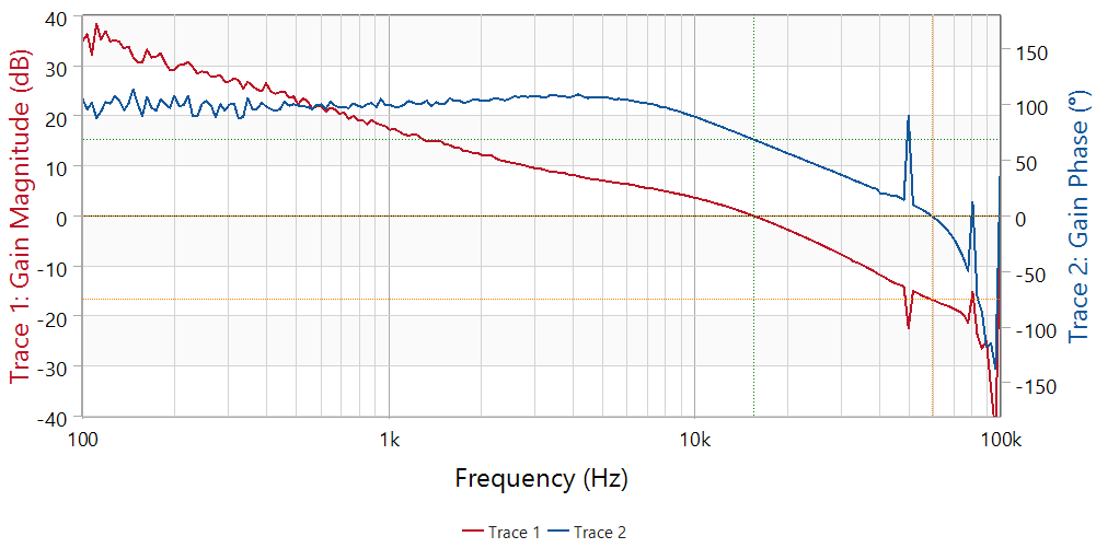
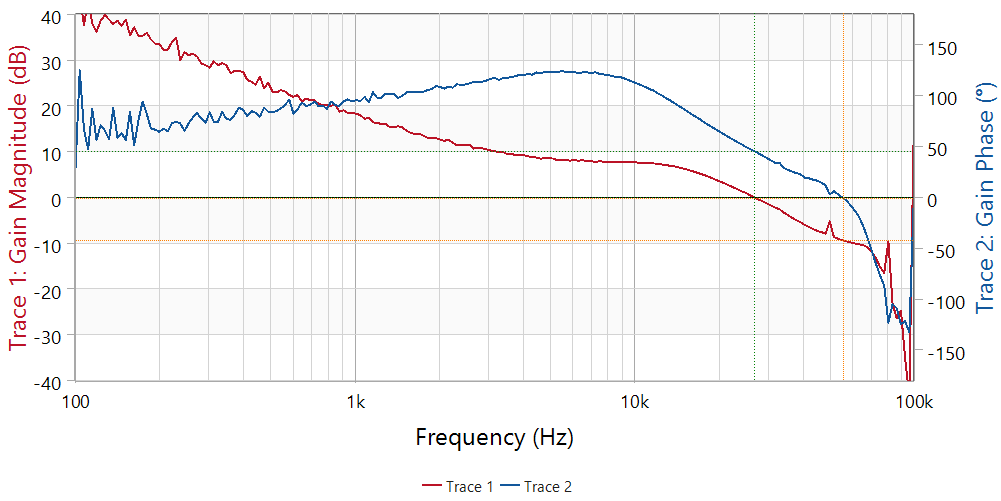
The feedback loop frequency response was measured with a 5-A load at different input voltage conditions and is shown in the following figures.
Table 2-4 Feedback Loop Frequency
Response
| Condition | Unity Gain Bandwidth (kHz) | Phase Margin (°) | Gain Margin (dB) |
|---|---|---|---|
| 50 VIN, 5-A load | 6.9 | 80 | 22.5 |
| 100 VIN, 5-A load | 15.6 | 69 | 17.7 |
| 150 VIN, 5-A load | 27 | 46 | 9.4 |
 Figure 2-6 Bode Plot, 50 VIN,
5-A Load
 Figure 2-7 Bode Plot, 100 VIN,
5-A Load
 Figure 2-8 Bode Plot, 150 VIN,
5-A Load