TIDUEY7 July 2021
- Description
- Resources
- Features
- Applications
- 5
- 1System Description
-
2System Overview
- 2.1 Block Diagram
- 2.2
Design Considerations
- 2.2.1 System Control and Processing
- 2.2.2 Analog Front End
- 2.2.3 Input Voltage Monitoring: 5 V, 20 V, 40 V, and ±5 V
- 2.2.4 Bidirectional Current Sense: ±2 A
- 2.2.5 Unipolar Current Sense: 0.25 A to 1 A
- 2.2.6 TMP461-SP: Local and Remote Temperature Sensing
- 2.2.7 NTC Thermistor Temperature Sensing
- 2.2.8 Adjustable Voltage Source
- 2.2.9 Fixed Output Current Source
- 2.2.10 Adjustable 4-mA Current Source
- 2.2.11 Power Tree and Power Sequencing
- 2.3 Highlighted Products
- 3Hardware, Software, Testing Requirements, and Test Results
- 4Design and Documentation Support
- 5About the Author
2.2.11 Power Tree and Power Sequencing
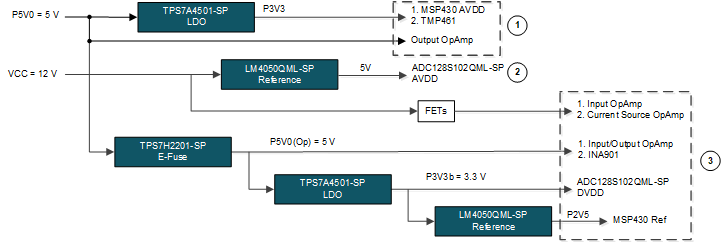
Figure 2-11 shows the power tree consisting of four main power components: the TS7A4501-SP, LMP4050QML-SP, TPS7H2201, and boost circuit.
 Figure 2-11 Power Tree and Sequencing
The TPS7A4501-SP is selected to power these rails because of its low noise output to ensure no performance degradation due to injected power noise. There are three TPS7A4501-SP used to power this design. The first TPS7A4501-SP provides a 3.3-V rail used to power the MSP430FR5969-SP. The second TPS7A4501-SP is used to provide the 3.3-V digital voltage rail for the ADC128S102QML-SP. The third device is used to regulate the output of the discrete boost controller to 12 V. The 12 V supplied by the TPS7A4501-SP is optional to the operation of this reference design and an external 12 V can be provided to bypass the boost and LDO circuit.
The LMP4050QML-SP are voltage references to provide a stable voltage at two places in the power tree. The first is the 5-V analog voltage rail for the ADC128S102QML-SP. The second rail is the 2.5-V reference for the integrated ADC in the MSP430FR5969-SP. It is important that this is a clean stable signal, or else it can cause inaccuracies in the measurements taken from the ADC.
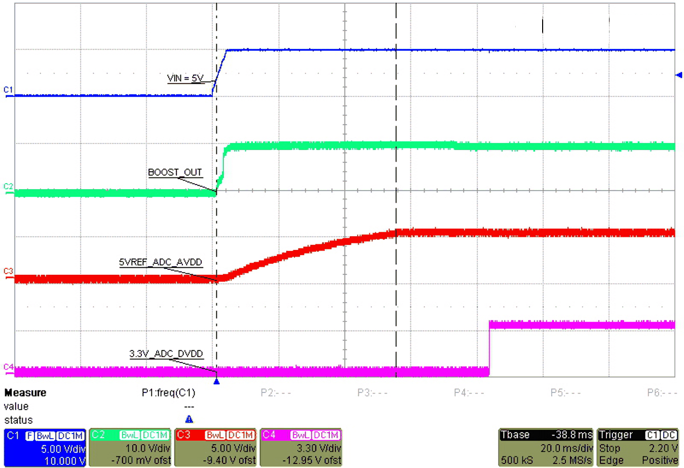
The TPS7H2201-SP is a load switch that is used for sequencing and ramp up power safely for the op amps. The main power sequencing in this design is to make sure that the ADC128S102QML-SP analog voltage rail has ramped up first before the digital voltage rails ramps up as Figure 2-12 shows. It is important that the analog voltage rail of the ADC128S102QML-SP is stable at 5 V, because the digital rail must stay at least 0.3 V below the analog voltage rail or else it could cause damage to the ADC128S102QML-SP.
 Figure 2-12 ADC128S102-SP Start-up Power Sequence