TIDUF04 December   2022


  1.   Description
  2.   Resources
  3.   Features
  4.   Applications
  5.   5
  6. 1System Description
    1.     7
    2. 1.1 EV Charging Station Challenges
      1. 1.1.1 SAE J1772 or Equivalent Standard Compliant EV Charging Stations
      2. 1.1.2 AC and DC Leakage, Residual Current Detection (RCD)
      3. 1.1.3 Efficient Relay and Contactor Drive
      4. 1.1.4 Contact Weld Detection
    3. 1.2 Key System Specifications
  7. 2System Overview
    1. 2.1 Block Diagram
    2. 2.2 Design Considerations
      1. 2.2.1 Isolated AC/DC Power Supply Design
        1. 2.2.1.1  Input Bulk Capacitance and Minimum Bulk Voltage
        2. 2.2.1.2  Transformer Turns-Ratio, Primary Inductance, and Primary Peak Current
        3. 2.2.1.3  Transformer Parameter Calculations: Primary and Secondary RMS Currents
        4. 2.2.1.4  Main Switching Power MOSFET Selection
        5. 2.2.1.5  Rectifying Diode Selection
        6. 2.2.1.6  Output Capacitor Selection
        7. 2.2.1.7  Capacitance on VDD Pin
        8. 2.2.1.8  Open-loop Voltage Regulation Versus Pin Resistor Divider, Line Compensation Resistor
        9. 2.2.1.9  Feedback Elements
        10. 2.2.1.10 Backup Power Supply
        11. 2.2.1.11 Supercapacitor Selection
        12. 2.2.1.12 Supercapacitor Charger Design
      2. 2.2.2 Control Pilot Signal Interface
        1. 2.2.2.1 J1772 Duty Cycle
          1. 2.2.2.1.1 Control Pilot Signal States
          2. 2.2.2.1.2 Control Pilot Signal Circuit
      3. 2.2.3 Relay Drive and Weld Detect
      4. 2.2.4 Residual Current Detection
        1. 2.2.4.1 Auto-Oscillation Circuit
          1.        37
        2. 2.2.4.2 DRV8220 H-Bridge
        3. 2.2.4.3 Saturation Detection Circuit
        4. 2.2.4.4 H-Bridge Controlled by DFF
        5. 2.2.4.5 Filter Stage
        6. 2.2.4.6 Differential to Single-Ended Converter
        7. 2.2.4.7 Low-Pass Filter
        8. 2.2.4.8 Full-Wave Rectifier
        9. 2.2.4.9 MCU Selection
    3. 2.3 Highlighted Products
      1. 2.3.1  UCC28742
      2. 2.3.2  TLV1805
      3. 2.3.3  DRV8220
      4. 2.3.4  ISO1212
      5. 2.3.5  ADC122S051
      6. 2.3.6  TPS7A39
      7. 2.3.7  TPS7A20
      8. 2.3.8  ATL431
      9. 2.3.9  TL431
      10. 2.3.10 TPS563210A
      11. 2.3.11 TPS55330
      12. 2.3.12 TPS259470
      13. 2.3.13 TL7705A
  8. 3Hardware, Testing Requirements, and Test Results
    1. 3.1 Hardware Requirements
    2. 3.2 Test Requirements
      1. 3.2.1 Power Supply Test Setup
      2. 3.2.2 Weld Detect Test Setup
    3. 3.3 Test Results
      1. 3.3.1 Isolated AC/DC Power Supply Based on UCC28742
        1. 3.3.1.1 Efficiency and Output Voltage Cross Regulation
        2. 3.3.1.2 Efficiency and Output Voltage Regulation of TPS563210
        3. 3.3.1.3 Output Voltage Ripple Waveforms
        4. 3.3.1.4 Start, Shutdown, Backup Power, and Transient Response Waveforms
        5. 3.3.1.5 Thermal Performance
      2. 3.3.2 TLV1805-Based Control Pilot Interface
        1. 3.3.2.1 TLV1805 Output Rise and Fall Time
        2. 3.3.2.2 Control Pilot Signal Voltage Accuracy in Different States
      3. 3.3.3 DRV8220-Based Relay and Plug Lock Drive
      4. 3.3.4 ISO1212-Based Isolated Line Voltage Sensing
  9. 4Design and Documentation Support
    1. 4.1 Design Files
      1. 4.1.1 Schematics
      2. 4.1.2 Bill of Materials
    2. 4.2 Documentation Support
    3. 4.3 Support Resources
    4. 4.4 Trademarks
  10. 5About the Author

Differential to Single-Ended Converter

The differential to single-end conversion is performed by the first part of the signal chain. The first op amp converts the differential signal across the fluxgate burden resistor to a single-ended signal. This simplifies later signal conditioning and allows the ADC to read a ground referenced signal. R22 is the burden resistor across the coils of the fluxgate sensor.

Impedance matching to op amp inputs is important to minimize error. Mismatched impedance adds error to the fault detection signal. Trace from R22 to U10 can be similar to reduce error. To increase the ground fault signal, replace R18 and R26 with buffer op amps or resistors an order of magnitude larger. A higher impedance relative to the burden resistor (R22) gives a higher ground fault signal due to the resistor divider effect.
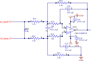
GUID-20220801-SS0I-FV8V-4L0Z-KZR8CBFGHL8Z-low.gifFigure 2-12 Differential to Single-Ended Schematic