TIDUF05 August 2022
- Description
- Resources
- Features
- Applications
- 5
- 1System Description
- 2System Overview
- 3Hardware, Testing Requirements, and Test Results
- 4Design and Documentation Support
- 5Documentation Support
- 6Support Resources
- 7Trademarks
2.2.2.2.1 Choosing External Components
For simplicity, the efficiency of the buck regulators is assumed to be 85% for these operating conditions, and the efficiency of the LDO is given by Equation 3.
System and Buck 1 currents calculated assuming 85% switching regulator efficiency are given in Equation 3.
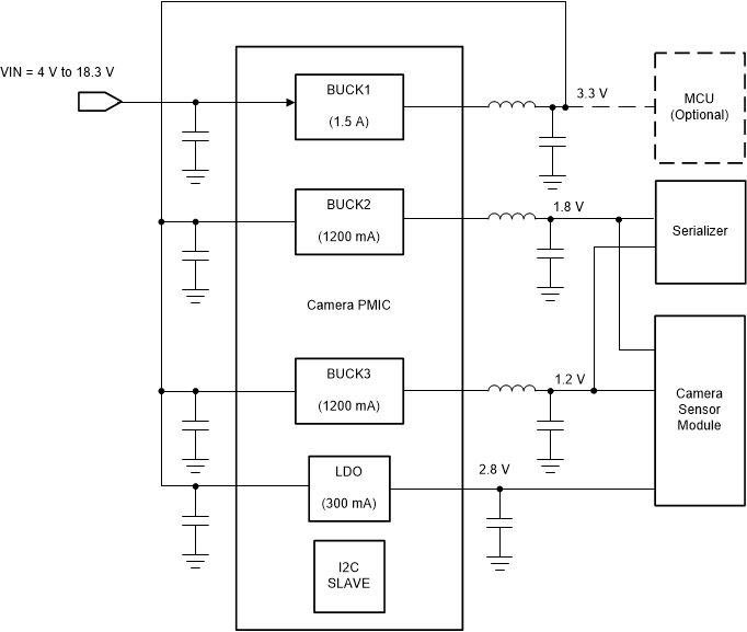
Table 2-2 shows the load capability of each regulator compared to the requirements of the camera module. The TPS650330-Q1 device is capable of supplying the system power with plenty of margin to account for variations between typical and maximum current variation.
| REGULATOR | OUTPUT VOLTAGE (V) | MAX CURRENT (mA) | REQUIRED CURRENT (mA) |
|---|---|---|---|
| Buck 1 | 3.3 | 1500 | 383 |
| Buck 2 | 1.8 | 1200 | 232 |
| Buck 3 | 1.2 | 1200 | 217 |
| LDO | 2.8 | 300 | 141 |
After determining that the TPS650330-Q1 device is suitable based on the power requirements, the external components can be chosen quickly based on the data sheet recommendations, simplifying the design process. These recommendations are shown in Figure 2-5 and Table 2-3.
 Figure 2-5 TPS650330-Q1 Typical
Application Circuit
Figure 2-5 TPS650330-Q1 Typical
Application Circuit| COMPONENT | DESCRIPTION | VALUE | UNIT |
|---|---|---|---|
| CVSYS,VSYS_S | VSYS and VSYS_S decoupling | 10 | µF |
| CPVIN_B1 | Buck 1 input capacitor | 10 | µF |
| LSW_B1 | Buck 1 inductor |
1.5 |
µH |
| COUT_B1 | Buck 1 output capacitor | 10 | µF |
| CPVIN_B2 | Buck 2 input capacitor | 10 | µF |
| LSW_B2 | Buck 2 inductor | 1.0 | µH |
| COUT_B2 | Buck 2 output capacitor | 10 | µF |
| CPVIN_B3 | Buck 3 input capacitor | 10 | µF |
| LSW_B3 | Buck 3 inductor | 1.0 | µH |
| COUT_B3 | Buck 3 output capacitor | 10 | µF |
| CPVIN_LDO | LDO input capacitor | 1.0 | µF |
| COUT_LDO | LDO output capacitor | 2.2 | µF |