SBAA290A May 2018 – May 2021 ADS1235 , ADS1261
Application Brief
Introduction
Many industrial end-equipment employ resistive bridges to sense changes in physical variables such as strain, force, pressure, temperature, or flow rates. A common industrial application for resistive bridges is precision weigh scales. In this application, weight is translated into a voltage using a resistive bridge embedded in a load cell similar to Figure 1-1.
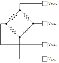 Figure 1-1 Resistive Bridge in a Load
Cell
Figure 1-1 Resistive Bridge in a Load
CellThe 4-wire load cell shown in Figure 1-1 requires an excitation voltage, VEXC±, and outputs a differential signal voltage, VSIG±, proportional to the applied weight. Typically, VSIG± (max) is on the order of tens of millivolts, requiring a low-noise, precision delta-sigma ADC with an integrated gain stage to provide repeatable measurements for such low-level signals.
ADC accuracy parameters such as offset error, offset drift, gain error and gain drift are important to ensure the weigh scale output correlates to the correct weight. To meet the demanding performance needs of precision bridge measurements, Texas Instruments offers the ADS1235, a 24-bit, 7.2-kSPS, 6-channel delta-sigma ADC, as well as the ADS1261, a 24-bit, 40-kSPS, 10-channel, delta-sigma ADC. Both of these ADCs incorporate several features necessary for precision bridge measurements, including:
- Integrated PGA – the ADS1261 provides all binary gains from 1 to 128 while the ADS1235 offers gain values of 1, 64, and 128, enabling input-referred noise as low as 6 nVRMS
- Differential voltage reference inputs – enables ratiometric measurements that provide the lowest-noise signal acquisition
- AC excitation control signals – use with external switches to swap bridge excitation polarity to reduce offset and offset drift
This document focuses on AC excitation to demonstrate why it is important and how it works using the ADS1235 and ADS1261. The subsequent sections only reference the ADS1235 because the same principles and operation generally apply to the ADS1261. However, should any relevant differences exist between these ADCs, they are noted.
What is AC Excitation?
While some ADCs, including the ADS1235, integrate chopping techniques to reduce device offset, these methods only reduce those errors that occur after the chopping circuitry. Therefore, any offset prior to the input of the device can still degrade measurement accuracy.
AC excitation, or bridge chopping, helps solve this design challenge by reducing system-level offset errors from a bridge measurement. Reducing the system offset also reduces system offset drift, an error term that is not easily removed by calibration.
The AC excitation method described in this document uses external switches to alternate the bridge excitation polarity, and should not be confused with excitation using a true AC signal. Instead, the system averages one forward-polarity and one reverse-polarity measurement to yield a single conversion result that is virtually offset-free.
Typical AC Excitation Circuit Using the ADS1235
Figure 1-2 depicts a simplified connection diagram for a typical 4-wire AC excitation circuit using the ADS1235.
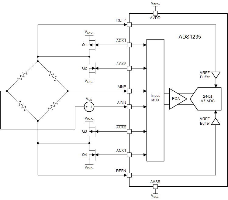 Figure 1-2 Four-Wire AC Excitation
Circuit Using ADS1235
Figure 1-2 Four-Wire AC Excitation
Circuit Using ADS1235Figure 1-2 employs two P-channel MOSFETs and two N-channel MOSFETs to forward and reverse bias the bridge. These MOSFETs are controlled by specific ADC pins: ACX1, ACX2, ACX1, and ACX2. The timing and logic levels of each signal must be tightly controlled to switch the MOSFETs effectively. Figure 1-3 shows the timing diagram for the ADS1235 ACX pins.
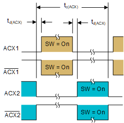 Figure 1-3 ADS1235 AC Excitation Signal
Timing Diagram
Figure 1-3 ADS1235 AC Excitation Signal
Timing DiagramThe orange highlights in Figure 1-3 denote when the MOSFETs (Q1 and Q4) are enabled during the forward-polarity phase, while the blue highlights indicate when the MOSFETS (Q2 and Q3) conduct during the reverse-polarity phase. Importantly, the delay, td(ACX), between the ON-time for each switch avoids any MOSFET shoot-through current that results if both a P-channel and N-channel device are on simultaneously.
The logic levels on the ADS1235 ACX pins are referenced to the ADC analog supply (AVDD), not the digital supply (DVDD) as some might expect, due to the following system factors:
- Resistive bridge measurements typically operate with VEXC = 5 V to maximize dynamic range
- AVDD on the ADS1235 is restricted to 5 V
- VEXC is commonly shared with AVDD and AVSS (see Figure 1-2) as long as doing so does not violate the ADC operating conditions
As a result of these three factors, the ACX pins must use 5-V logic levels to sufficiently control the MOSFETs in the system shown in Figure 1-2, which is why these pins are referenced to AVDD.
How does AC excitation improve system accuracy?
AC excitation averages two consecutive measurements, VPHASE1 and VPHASE2, to remove offset error. Equation 1 calculates the combined conversion result.
Figure 1-4 shows the connection diagrams and the excitation voltage path for both the Phase 1 (Figure 1-4A) and Phase 2 (Figure 1-4B) measurements.
 Figure 1-4 AC Excitation Connection
Diagrams: Phase 1 (Left) and Phase 2 (Right)
Figure 1-4 AC Excitation Connection
Diagrams: Phase 1 (Left) and Phase 2 (Right)In Phase 1 of the AC excitation mode of the ADS1261 (see Figure 1-4A), the ACX1 and ACX1 outputs are enabled such that VEXC+ connects to the top of the bridge and VEXC- connects to the bottom of the bridge. As highlighted in orange in the timing diagram in Figure 1-3, ACX1 is at logic low (0 V) and ACX1 is at logic high (5 V) during the forward-polarity phase. With ACX1 at 0 V, the gate-source voltage, VGS, is < 0 V, which turns Q1 on. Similarly, ACX1 at 5 V sets VGS > 0 for Q4, which turns Q4 on as well. The opposite is true for Q2 and Q3 such that both of these devices do not conduct.
Equation 2 shows VPHASE1 in terms of VSIG± as well as the offset term, VOS, which represents all offsets in the measurement system.
In Phase 2, the ACX outputs switch such that only the MOSFETs connected to ACX2 and ACX2 conduct. This configuration routes VEXC+ to the bottom of the bridge and VEXC– to the top, reversing the polarity of the signal seen at the inputs of the ADC (AINN and AINP). Figure 1-4B shows this reverse-polarity configuration.
As highlighted in blue in the timing diagram in Figure 1-3, ACX2 is at logic low (0 V) and ACX2 is at logic high (5 V) during the reverse-polarity phase. With ACX2 at 0 V, VGS is < 0 V, which turns Q2 on. Similarly, ACX2 at 5 V sets VGS > 0 for Q3, which turns Q3 on as well. The opposite is true for Q1 and Q4 such that both of these devices do not conduct.
In the reverse-polarity configuration shown in Figure 1-4B, VPHASE2 is represented by Equation 3. Note that while the measurement polarity is reversed, the bridge offset polarity is the same.
Replacing VPHASE1 and VPHASE 2 from Equation 1 with Equation 2 and Equation 3, respectively, yields VCONV_RESULT in terms of VSIG± and VOS as shown in Equation 4.
Reducing Equation 4 and combining similar terms yields a final conversion result (Equation 5) that is independent of VOS, which is the desired outcome.
Two-Wire versus Four-Wire AC Excitation
While the previous section shows how to implement AC excitation using all four ACX pins on the ADS1235, it is possible to use only two of the ACX pins to implement AC excitation. Figure 1-5 shows the modifications required to implement 2-wire AC excitation using the ADS1235.
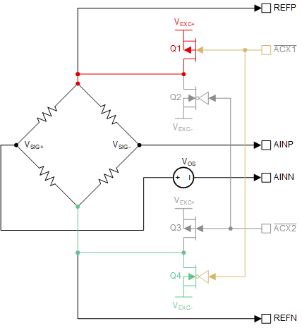 Figure 1-5 Phase 1 Connection Diagram
for 2-Wire AC Excitation
Figure 1-5 Phase 1 Connection Diagram
for 2-Wire AC ExcitationIn Figure 1-5, only the ACX1 and ACX2 pins are used. ACX1 is connected to Q1 and Q4 while ACX2 is connected to Q2 and Q3. The addition of two inverters on Q2 and Q4 effectively mimics the 4-wire timing diagram behavior shown in Figure 1-3. For example, Figure 1-3 shows that when ACX1 is in the forward-polarity, on-switch position, ACX1 is logic low. This turns Q1 on, while at the same time the inverted input (logic high) is applied to Q4, turning this MOSFET on as well.
While not shown, the 2-wire AC excitation reverse-polarity phase is the behavioral opposite of the forward polarity phase, similar to the 4-wire case (see Figure 1-4B). Moreover, the phase and conversion result equations are the same as described in the previous section.
Example AC Excitation Circuit on the ADS1235 EVM
The ADS1235 evaluation module (EVM) includes an AC excitation circuit that uses a dual-channel gate driver instead of individual MOSFETs to control the bridge. The gate driver used on the EVM is the Texas Instruments UCC27524, a non-inverting device, though it is possible to use the inverting UCC27523 as well. The block diagrams for both devices are shown in Figure 1-6.
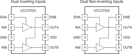 Figure 1-6 UCC27523 (Inverting) and
UCC27524 (Non-inverting) Block Diagrams
Figure 1-6 UCC27523 (Inverting) and
UCC27524 (Non-inverting) Block DiagramsThe UCC27524 operates by driving its OUTx pins to the supply voltage (VDD) when a logic-high input (≥ 2.1 V typical) is applied to INx, or to GND when a logic-low input (≤ 1.2 V typical) is applied to INx. The INx pin voltages are independent of VDD, enabling a dedicated VEXC± that can be greater than the maximum AVDD of 5 V for the ADS1235. This can be used to improve bridge dynamic range if VEXC±= VDD = 10 V for example, though there is a tradeoff of higher power consumption and potential sensor self-heating. Moreover, take care to ensure that any voltages applied to the ADC are within the specified operating conditions.
Figure 1-7 shows the portion of the EVM schematic that contains the AC excitation circuitry, including the UCC27524.
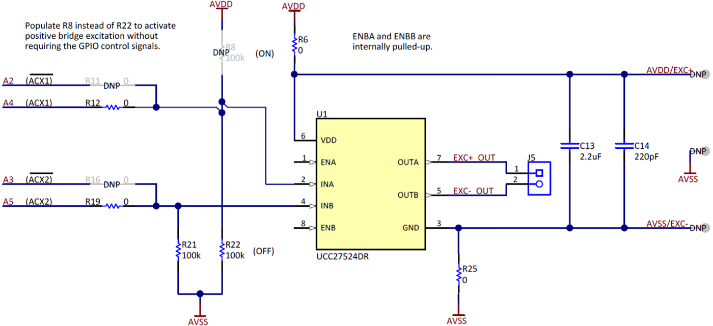 Figure 1-7 AC Excitation Circuit on the
ADS1235 EVM
Figure 1-7 AC Excitation Circuit on the
ADS1235 EVMAs Figure 1-7 shows, only two of the four ACX pins are required to implement AC excitation on the ADS1235 EVM. ACX1 and ACX2 are used with the non-inverting UCC27524 that comes standard on the EVM. Comparatively, ACX1 and ACX2 are used if the UCC27524 is replaced with the inverting UCC27523, which also requires adding resistors R11 and R16 and removing R12 and R19. In either case, the gate driver output is connected to J5-1 and J5-2, which in turn are connected to VEXC+ and VEXC–, respectively, on an external bridge.
During the forward polarity phase in the circuit in Figure 1-7, ACX1 is at logic high and ACX2 is at logic low, which sets VEXC+ to AVDD and VEXC– to GND, respectively. During the reverse-polarity phase of the measurement, ACX1 is at logic low and ACX2 is at logic high, which sets VEXC+ to GND and VEXC– to AVDD, respectively. Refer to the timing diagram in Figure 1-3 for more information on the logic levels of each pin during each phase.
After each phase is complete, the ADS1235 takes one measurement and then automatically averages both measurements together pursuant to Equation 2 through Equation 5. The ADS1235 EVM GUI then provides one conversion result with the system-level offset effectively removed.
Simplifying AC Excitation with the ADS1235
While the AC excitation control circuitry integrated into the ADS1235 can drive external switching components to reverse the polarity of the bridge, this ADC offers additional features to ensure reliable operation.
For example, Phase 2 reverses the excitation voltages such that VEXC+ and VEXC– are connected to REFN and REFP, respectively, resulting in a negative differential reference voltage, VREF (see Figure 1-4B). Since the ADS1235 cannot support a negative VREF, the ADC automatically reverses REFP and REFN during Phase 2 such that a positive VREF is always applied to the ADC. Using an ADC without this functionality requires manual VREF reversal.
As was discussed previously, the ADS1235 operation also ensures non-overlapping output drive signals, avoiding any MOSFET shoot-through current that could result if both a P-channel and N-channel device were on at the same time (refer to td(ACX) in Figure 1-3). Moreover, the AC excitation chop rate is synchronized to the conversion data rate to avoid unnecessarily fast switching.
Additional Considerations for AC Excitation
As with any additional circuitry added to a system, there is a performance tradeoff associated with implementing AC excitation: the improvement in system accuracy requires two measurements to generate one conversion result, thereby increasing conversion time. This doubles the conversion latency values shown in the Conversion Latency table in the ADS1235 Precision, 3-Channel, Differential-Input, 7200-SPS, 24-Bit Delta-Sigma ADC for Bridge Sensors data sheet when AC excitation is enabled. Fortunately, this latency only applies to the first conversion, as subsequent conversions average the previous result with the current result to provide the chopped output value.
Moreover, an added benefit of AC excitation is that the averaging of two measurements reduces the noise performance by a factor of √2. Therefore, the noise values in the Noise and Effective Resolution table in the ADS1235 data sheet can be divided by 1.41 when AC excitation is enabled.
Conclusion
Bridge measurements require both precise and accurate systems. The ADS1235 and ADS1261 from Texas Instruments are low-noise, high-accuracy delta-sigma ADCs that integrate control signals for AC excitation circuitry to help reduce system-level offset and offset drift.