SBAA573 February 2023 TRF1108 , TRF1208 , TRF1208B
1 Application Brief
Introduction
The Xilinx RFSoC platform integrates up to 16 high-speed RF-sampling data converter devices. The data converters support signal frequencies up to 7 GHz and beyond. With this level of channel integration in one device, a traditional passive balun interface coupled with a gain stage presents an issue with physical board space. It is challenging to place the all of the components close to the data converter pins with so many channels. Further, transformers and baluns are traditionally narrow band. So, while the data converter devices support a wide frequency range, the actual design becomes limited by the bandwidth performance of the balun.
Texas Instruments’ TRF1208 and TRF1108 devices introduce a broadband active balun. The TRF1208 supports single-ended to differential conversion for the ADC interface. The TRF1108 supports the differential to single-ended conversion with higher output power capability for the transmitter device. These devices are small (2 × 2 mm) and are on-par with some of the smallest passive baluns on the market. More importantly, the devices are broadband, operating up to almost 12 GHz. With this one interface, all frequency bands can be supported without modifying the primary components. Only a few passive matching components can be modified if needed to optimize the interface for a specific frequency or layout topography.
This report completes the simulation interface using the published S-parameters of the respective device to demonstrate the performance expectation between the TRF1x08 and the Xilinx RFSoC. The simulations use ADS circuit simulations from Agilent®. The simulations include a realistic interconnect topology to account for the real-world trace lengths required to connect the devices together. The Xilinx RFSoC S-parameters are reflective of the ZCU670 development board. The parameters are available through the Xilinx web page. The TRF1x08 S-parameters are available from the TI web page on their respective product pages.
RFSoC Receiver
#GUID-5B725335-9F32-4938-A86C-8767ABF96808 shows the receiver circuit topology including the interconnecting traces. The goal is to represent a compact design using 0201-size passive components. By default, the differential traces are close together. The differential traces are modeled as coupled lines with specified width and spacing to maintain a 100-Ω differential impedance. The substrate is defined with an 8-mil height and a dielectric constant of 4.1. The height is kept in the 8- to 10-mil range to keep trace widths relatively small but provide sufficient spacing from the top layer to the ground layer to minimize plane capacitance which artificially rolls-off performance at higher frequencies.
The capacitor model is a standard ideal element. An S-parameter model for a real capacitor can be used, if desired, for high operation frequencies. Use a high-quality, high-frequency microwave capacitor like the AVX AccuP series for the high-frequency matching circuits. The inductor element is a pure inductor with an included parameter for the loss factor Q. Similarly, a device-specific S-parameter file for a specific inductor can be used here. A high-quality microwave inductor like the Murata® LQP03 series work well at the high frequencies.
 Figure 1-1 RFSoC Receiver Simulation
Circuit Diagram
Figure 1-1 RFSoC Receiver Simulation
Circuit DiagramSeries resistors R7 and R8 provide a small amount of series resistance to maintain stable operation of the amplifier. Capacitors C5 and C6 are DC blocking caps; select their values based on the operating frequency. Components C1 and C2 and L3 and L4 represent the matching circuit. In addition to matching, the combination of L3 and L4 with C1 provide an L-C low-pass anti-aliasing filter to attenuate broadband noise or spurs from the amplifier output. The trace lengths for the interconnects represent minimum lengths to connect 0201-sized components while maintaining sufficient keep-out spacing needed for pick-n-place manufacturing.
#GUID-A5DFE172-C41A-4D8C-B640-24074223D336 shows a representation of the physical layout per the simulations.
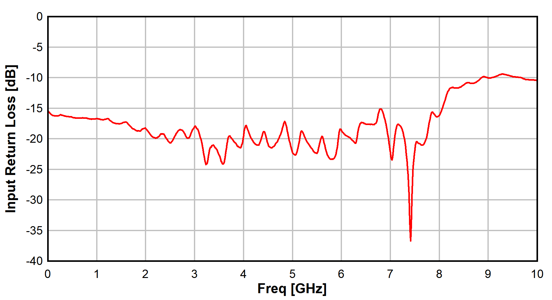
The goal of the simulation is to achieve good broadband return loss performance, paying particular attention to the performance up to 7-GHz band where the parasitics of the devices (and board) begin to noticeably impact and degrade the overall performance. The simulation is swept from 1 GHz to 10 GHz, which is the limit of the frequency available in the S-parameter file for the RFSoC. At low frequency, the performance is good; in these bands there is no need for specific matching components. The devices can be simply cascaded together with proper AC coupling cap and anti-aliasing filer. At higher frequencies, around 7 GHz, the matching components improve performance. #GUID-05FA1D2C-00AC-47F2-9C73-A237A8D3406D shows the simulated return loss performance with the matching topology and values from the simulation schematic.
 Figure 1-3 Composite RX Return Loss
Performance
Figure 1-3 Composite RX Return Loss
PerformanceThe composite return loss performance is mostly better than –15 dB through 8 GHz and better than –10 dB out to 10 GHz.
RFSoC Transmitter
A similar analysis on the transmitter uses the RF-DAC S-parameters of the Xilinx RFSoC and the TRF1108 transmitter active balun. For the transmit side, there is not a filtering concern between the DAC and amplifier. Appropriate filtering is included further down the transmit line-up. The output differential impedance of the DAC is inherently good as is the differential input to the TRF1108 amplifier. There is minimal need for matching circuits between the two. Correspondingly, a few of the components can be eliminated as compared to the RX case to streamline the output topology. The interface circuit keeps a small shunt capacitor close to the pins of the DAC device, a series coupling capacitor, and a series resistor. The single-ended output impedance of the TRF1108 deviates from 50 Ω at higher frequencies. This design is focused on operation through 7 GHz. The output port is matched with a shunt capacitance to improve return loss at that frequency. #GUID-BB36B7B1-3895-44EA-8219-5053A71CA5A5 shows the transmitter circuit topology and #GUID-3251AD60-2ECC-4761-A052-DF2ED4A3FB70 shows a representation of the physical layout between the RF-DAC and differential amplifier input.
 Figure 1-4 RFSoC Transmitter Simulation
Circuit Diagram
Figure 1-4 RFSoC Transmitter Simulation
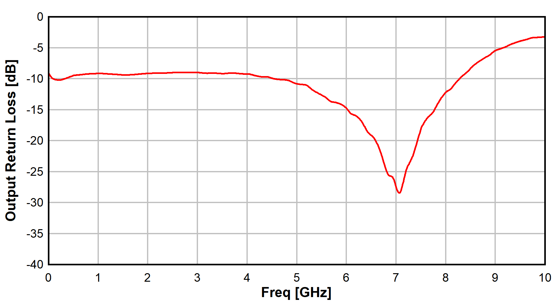
Circuit DiagramSimilar to the receiver case, the simulation frequency is swept from 1 GHz to 10 GHz. #GUID-E37C1B1B-2A9B-415A-9FC2-06C63B12858F shows the output return loss. The return loss is primarily dictated by the S22 performance of the amplifier. With the match component, the output return loss yields better than 10 dB from 5 to 8 GHz and is optimized at 7 GHz. A tweaking of the output capacitor shifts the optimized point slightly. Because of the amplifier isolation between the input and the output, match modifications between the RF-DAC and amplifier input do not impact the output return loss significantly. That is another way of saying that the amplifier is working as a good buffer device. #GUID-E37C1B1B-2A9B-415A-9FC2-06C63B12858F shows the return loss performance with an amplifier match in place.
 Figure 1-6 Composite TX Return Loss
Performance
Figure 1-6 Composite TX Return Loss
PerformanceConclusion
Each of the respective devices inherently have good broadband impedance performance. As expected, there is degradation at higher frequencies due to internal parasitic elements in the design and package. With proper matching, performance improves at the higher frequency of interest.
Each design is different. The simulations in this report are intended to be used as a guide. Each layout has a different PCB stack-up configuration which impacts the trace width to maintain the desired characteristic impedances. There can be other factors that dictate trace length in the design. The circuit topology can be used and modified for any specific configuration to get a close approximation. The topology offers placeholders for appropriate matching components that facilitate minor adjustments once actual board measurements are taken into account for unpredictable variations in the PCB board or inaccuracies within the models.
References
- Xilinx Incorporated, UltraScale Architecture PCB Design User Guide, Retrieved from https://docs.xilinx.com/r/en-US/ug583-ultrascale-pcb-design/UltraScale-Architecture-PCB-Design-User-Guide
- Xilinx Incorporated, ZCU670 Evaluation Board User Guide (UG1532), Retrieved from https://docs.xilinx.com/r/en-US/ug1532-zcu670-eval-bd/Zynq-UltraScale-RFSoC-XCZU67DR