SBOA247A december 2018 – april 2023 OPA376 , TLV9002
Design Goals
| Input ViDiff(Vi2 – Vi1) | Output | Supply | ||||
|---|---|---|---|---|---|---|
| ViDiff_Min | ViDiff_Max | VoMin | VoMax | Vcc | Vee | Vref |
| –2.22 mV | 2.27 mV | 225 mV | 4.72 V | 5 V | 0 V | 2.5 V |
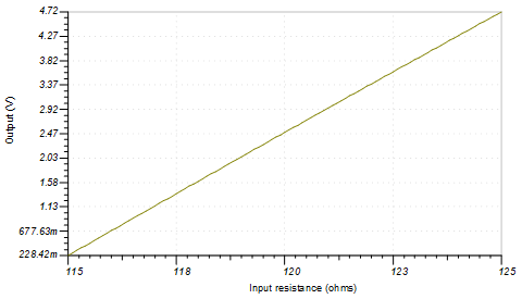
| Strain Gauge Resistance Variation (R10) | Vcm | Gain |
|---|---|---|
| 115 Ω – 125 Ω | 2.39 V | 1001 V/V |
Design Description
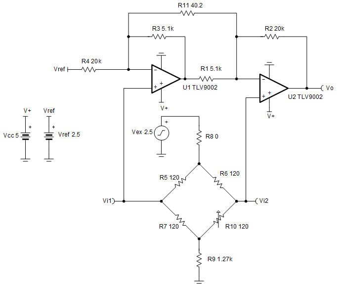
A strain gauge is a sensor whose resistance varies with applied force. The change in resistance is directly proportional to how much strain the sensor is experiencing due to the force applied. To measure the variation in resistance, the strain gauge is placed in a bridge configuration. This design uses a two op amp instrumentation circuit to amplify a differential signal created by the change in resistance of a strain gauge. By varying R10, a small differential voltage is created at the output of the Wheatstone bridge which is fed to the two op amp instrumentation amplifier input. Linear operation of an instrumentation amplifier depends upon the linear operation of the primary building block: op amps. An op amp operates linearly when the input and output signals are within the input common-mode and output-swing ranges of the device, respectively. The supply voltages used to power the op amps define these ranges.
Design Notes
- Resistors R5, R6, and R7 of the Wheatstone bridge must match the stain gauge nominal resistance and must be equal to avoid creating a bridge offset voltage.
- Low tolerance resistors must be used to minimize the offset and gain errors due to the bridge resistors.
- Vex sets the excitation voltage of the bridge and the common-mode voltage Vcm.
- Vref biases the output voltage of the instrumentation amplifier to mid-supply to allow differential measurements in the positive and negative directions.
- R11 sets the gain of the instrumentation amplifier circuit.
- R8 and R9 set the common-mode voltage of the instrumentation amplifier and limits the current through the bridge. This current determines the differential signal produced by the bridge. However, there are limitations on the current through the bridge due to self-heating effects of the bridge resistors and strain gauge.
- Make sure that R1 = R3 and R2 = R4 and that ratios of R2/R1 and R4/R3 are matched to set the Vref gain to 1 V/V and maintain high DC CMRR of the instrumentation amplifier.
- Linear operation is contingent upon the input common-mode and the output swing ranges of the op amps used. The linear output swing ranges are specified under the Aol test conditions in the op amps data sheets.
- Using high-value resistors can degrade the phase margin of the circuit and introduce additional noise in the circuit.
Design Steps
- Select R5, R6
and R7 to match the stain gauge nominal resistance
- Choose R9 to set the
common mode voltage of the instrumentation amplifier at 2.39 V
- Calculate the gain required to
produce the desired output voltage swing
- Select R1,
R2, R3, and R4. To set the Vref gain
at 1 V/V and avoid degrading the instrumentation amplifier’s CMRR, R1
must equal R3 and R2 must equal R4.
- Calculate R11 to meet
the required gain
- Calculate the current through the
bridge
Design Simulations
DC Simulation Results
References
- Analog Engineer's Circuit Cookbooks
- SPICE Simulation File SBOMAU4
- TI Precision Designs TIPD170
- TI Precision Labs
- VCM vs. VOUT plots for instrumentation amplifiers with two op amps
| TLV9002 | |
|---|---|
| Vss | 1.8 V to 5.5 V |
| VinCM | Rail-to-rail |
| Vout | Rail-to-Rail |
| Vos | 0.4 mV |
| Iq | 0.06 mA |
| Ib | 5 pA |
| UGBW | 1 MHz |
| SR | 2 V/µs |
| #Channels | 1, 2, and 4 |
| TLV9002 | |
Design Alternate Op Amp
| OPA376 | |
|---|---|
| Vss | 2.2 V to 5.5 V |
| VinCM | (Vee – 0.1 V) to (Vcc – 1.3 V) |
| Vout | Rail-to-Rail |
| Vos | 0.005 mV |
| Iq | 0.76 mA |
| Ib | 0.2 pA |
| UGBW | 5.5 MHz |
| SR | 2 V/µs |
| #Channels | 1, 2, and 4 |
| OPA376 | |