SBOA283 March 2021 LMV861 , OPA377 , TLV9002
Design Goals
| Input | Output | BW | Gain | Supply | |||
|---|---|---|---|---|---|---|---|
| ViMin | ViMax | VoMin | VoMax | fp | G | Vcc | Vee |
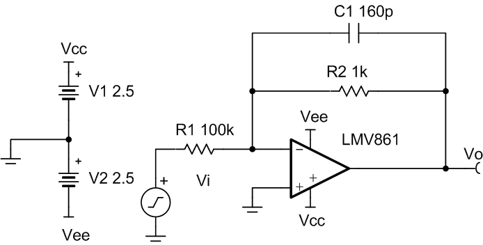
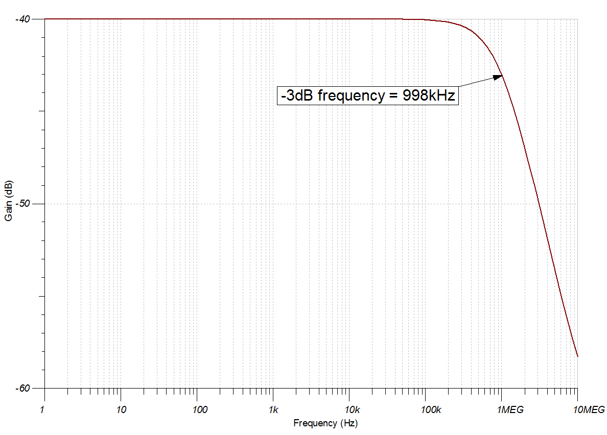
| –200V | 200V | –2V | 2V | 1MHz | –40dB | 2.5V | –2.5V |
Design Description
This circuit inverts the input signal, Vi, and applies a signal gain of –40dB. The common-mode voltage of an inverting amplifier is equal to the voltage applied to the non-inverting input, which is ground in this design.
Design Notes
- The common-mode voltage in this circuit does not vary with input voltage.
- The input impedance is determined by the input resistor. Make sure this value is large when compared to the output impedance of the source.
- Using high-value resistors can degrade the phase margin of the circuit and introduce additional noise in the circuit. The capacitor in parallel with R2 provides filtering and improves stability of the circuit if high-value resistors are used for both the input and feedback resistances.
- Avoid placing capacitive loads directly on the output of the amplifier to minimize stability issues.
- Small-signal bandwidth is determined by the noise gain (or non-inverting gain) and op amp gain-bandwidth product (GBP).
- Large signal performance may be limited by slew rate. Therefore, check the maximum output swing versus frequency plot in the data sheet to minimize slew-induced distortion.
- For more information on op amp linear operating region, stability, slew-induced distortion, capacitive load drive, driving ADCs, and bandwidth see the Design References section.
- Note that higher input voltage levels may require the use of multiple resistors in series to help reduce the voltage drop across the individual resistors. For more information, see the Design References section.
Design Steps
The transfer function of this circuit follows:
- Calculate the gain required for the
circuit. Equation 1.
- Choose the starting value of
R1. Equation 1.
- Calculate for a desired signal
attenuation of 0.01 V/V. Equation 1.
- Select the feedback capacitor, C1, to
meet the circuit bandwidth. Equation 1.
- Calculate the minimum slew rate
required to minimize slew-induced distortion. Equation 1.
- SRLMV861 = 18V/µs; therefore, it meets this requirement.
- Calculate the circuit bandwidth to ensure it meets
the 1-MHz requirement. Be sure to use the noise gain, NG, or non-inverting gain,
of the circuit. Equation 1.
- BWLMV861 = 30MHz; therefore, it meets this requirement.
- If C1 is not used to
limit the circuit bandwidth, to avoid stability issues ensure that the zero
created by the gain setting resistors and input capacitance of the device is
greater than the bandwidth of the circuit. Equation 1.
- Ccm and Cdiff are the common-mode and differential input capacitance of the LMV861, respectively.
Design Simulations
DC Simulation Results
AC Simulation Results
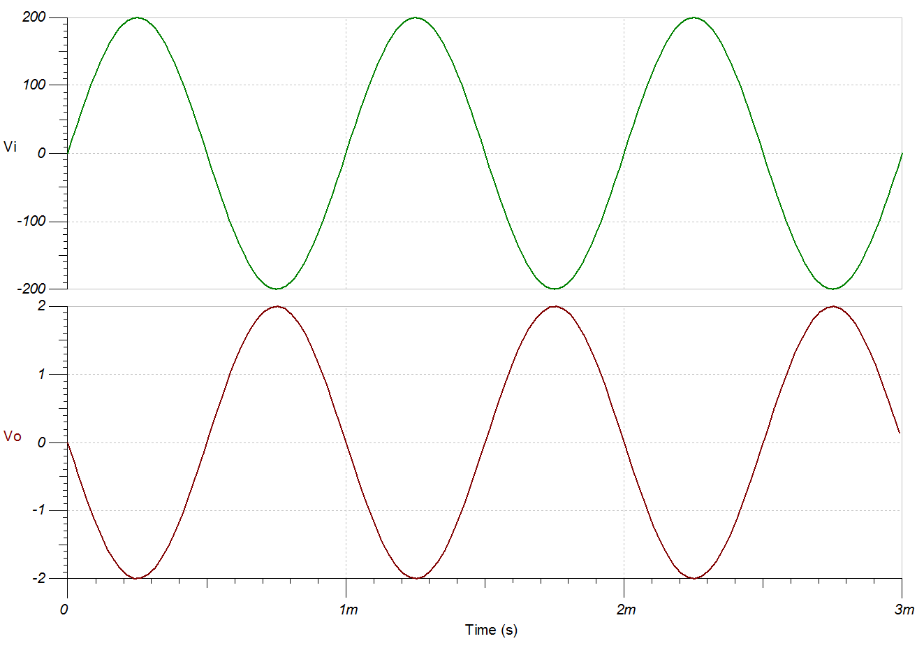
Transient Simulation Results
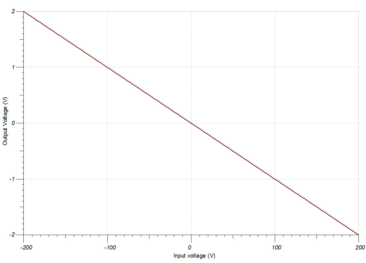
A 1-kHz, 400-Vpp input sine wave yields a 4-Vpp output sine wave.
Design References
- See Analog Engineer's Circuit Cookbooks for the comprehensive TI circuit library.
- SPICE Simulation File SBOC522.
- TI Precision Labs
- For more information on circuits with larger input voltages, see Considerations for High-Voltage Measurements.
Design Featured Op Amp
| LMV861 | |
|---|---|
| Vss | 2.7V to 5.5V |
| VinCM | (Vee – 0.1V) to (Vcc – 1.1V) |
| Vout | Rail-to-rail |
| Vos | 0.273mV |
| Iq | 2.25mA |
| Ib | 0.1pA |
| UGBW | 30MHz |
| SR | 18V/µs |
| #Channels | 1, 2 |
| www.ti.com/product/LMV861 | |
Design Alternate Op Amp
| TLV9002 | OPA377 | |
|---|---|---|
| Vss | 1.8V to 5.5V | 2.2V to 5.5V |
| VinCM | Rail-to-rail | Rail-to-rail |
| Vout | Rail-to-rail | Rail-to-rail |
| Vos | 0.4mV | 0.25mV |
| Iq | 0.06mA | 0.76mA |
| Ib | 5pA | 0.2pA |
| UGBW | 1MHz | 5.5MHz |
| SR | 2V/µs | 2V/µs |
| #Channels | 1, 2, 4 | 1, 2, 4 |
| www.ti.com/product/TLV9002 | www.ti.com/product/OPA377 |