SBOA529 October 2021 INA293 , INA293
Design Goals
The design goal is the realization of a bidirectional current sensing circuit with a unidirectional current sense amplifier.
| Input | Output | Supply |
Error |
|||
|---|---|---|---|---|---|---|
| IMin | IMax | Vout, min | Vout, max | Vcc | Vee | Over input current range |
| –10 A | +10 A | About 100 mV | About 4 V | 5 V | 0 V | ≤ 3% at room temperature ≤ 5% from 0°C to 85°C |
Design Description
This design utilizes a unidirectional current shunt monitor to measure a bidirectional load current. This concept only works for low-side current sensing applications. The load current range is from –10 A to +10 A, the output range is from 100 mV to 4 V, and the supply voltages are 5 V and ground.
Design Notes
- Analyze unidirectional current measurement circuit
- Change the circuit to measure
bidirectional current.
Use 0.1% tolerance resistors for R1 and R2 with a temperature coefficient of 10 ppm. An example, is the TNPW0603e3 resistor from Vishay® - Error calculation over input current and temperature
- As an example, the INA293A1 amplifier is used in this design note, but the concept is valid for many different current shunt monitors with input-bias-current information available and capable of low-side measurement
- Be sure to Kelvin-connect the shunt resistor
- Conduct a 1-point offset calibration at 25°C to compensate for resistor tolerances
Design Steps
- Unidirectional current
measurement standard circuit:
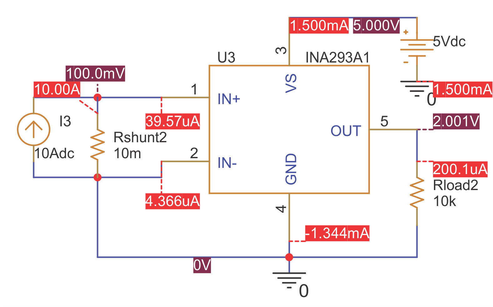
Standard Unidirectional Current Sensing - PSpice® for TI SimulationReversing the current in the previous example results in a negative voltage at the IN+ pin of the INA293A1 which will not disturb the part but results in an output voltage close to 0 V.
- Biasing the input voltage of the
INA293A1 by 100 mV makes it possible to measure a bidirectional current from –10
A to 10 A with an input voltage from about 0 to 200 mV and an output voltage
from close to 0 V to 4 V:
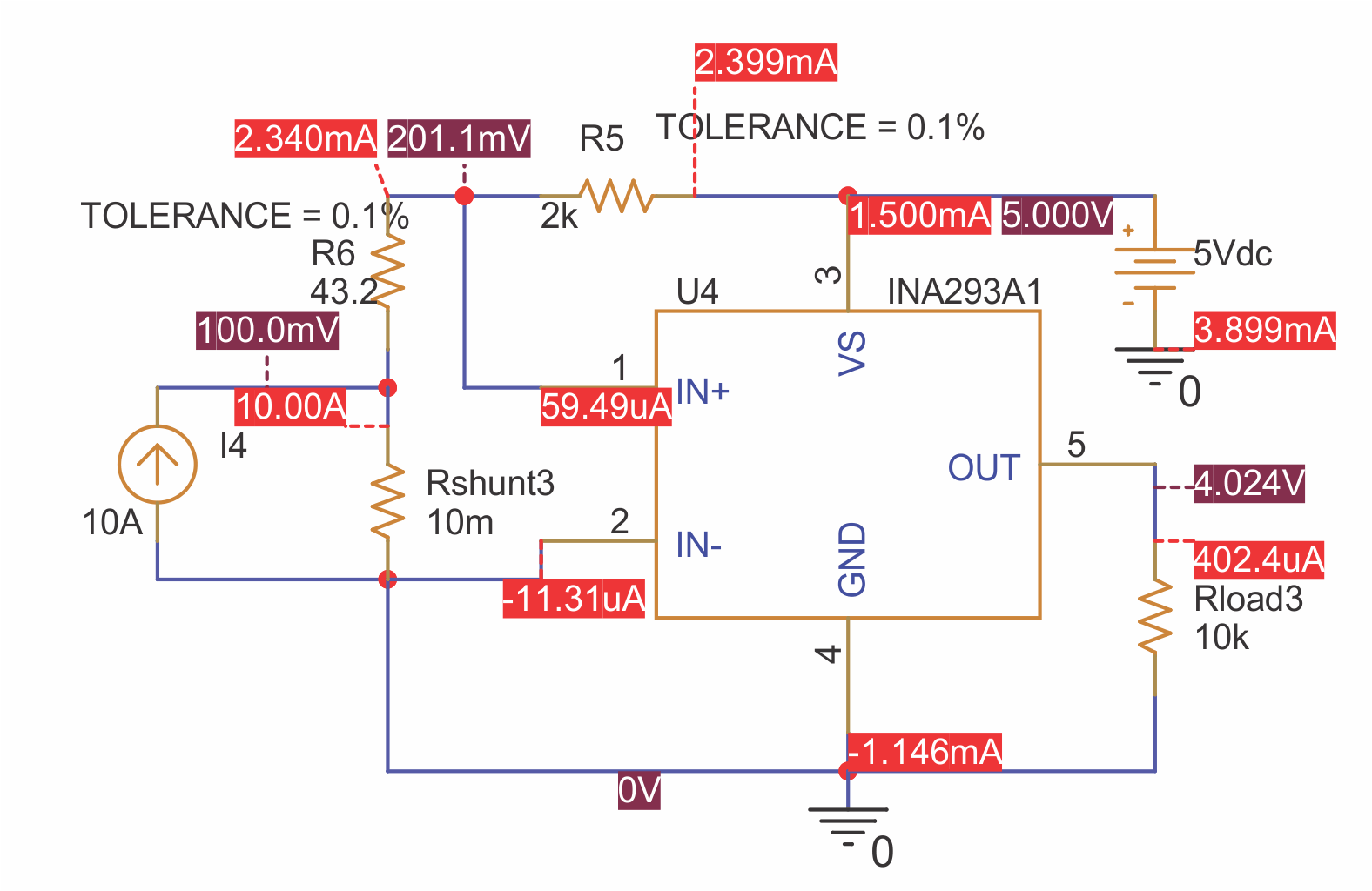
Modified Circuit With Biased Shunt Monitor Input VoltageChoosing R1 with 2 kΩ results in an error current of Ierror = (5 V – 0.201 V) / 2 kΩ = 2.4 mA which can be compensated after digitization in µC SW. To calculate R2, the input bias current of the INA293A1 must be considered. The input bias current into IN+ is taken from the data sheet: At 200 mV the current is typically about 60 µA (see the red dotted lines in INA239x1 Input Bias Current vs VSENSE), but could vary by ±20%. The simulation in the previous circuit shows the typical value. Because the IN– pin is connected to ground, this current can be ignored.
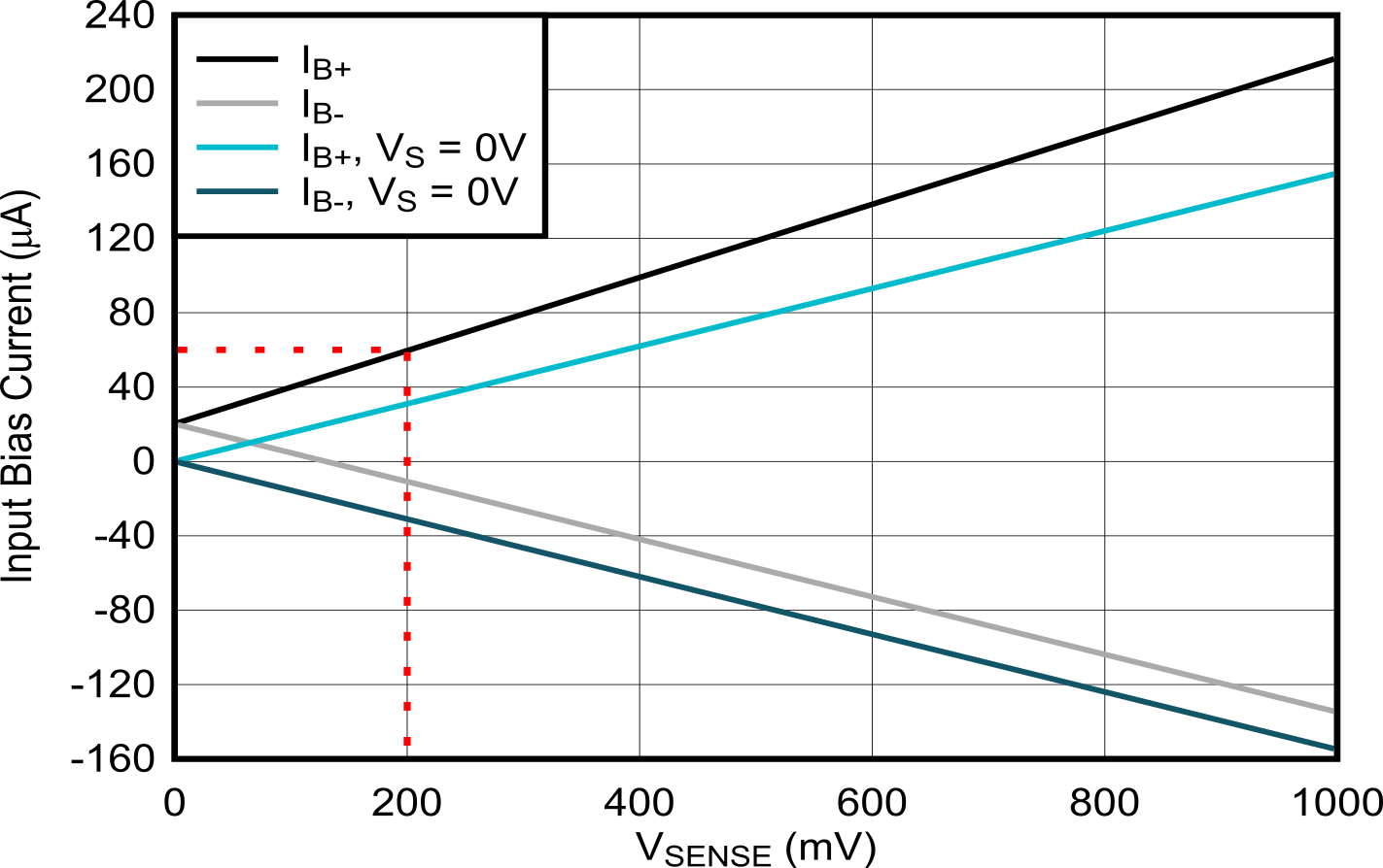
INA239x1 Input Bias Current vs VSENSER2 = 100 mV / (2.4 mA – 60 µA) = 42.7 Ω. The closest E96 value is 43.2 Ω which results in a slightly higher input voltage of 201.1 mV as the Error Calculations R1 MAX R2 MIN simulation shows. Choosing the higher value for R2 will also prevent the input going negative in case a current of –10 A is applied.
- R1 and R2 are the only additional error contributors compared to a unidirectional measurement. To get the worst-case values for the input voltage of the current shunt monitor in the Error Calculations R1 MAX R2 MIN schematics, a DC sweep from –10 A to +10 A is performed using PSPICE-FOR-TI.
Design Results
To calculate the worst-case error over temperature, check these two scenarios:
- R1max in combination with
R2min
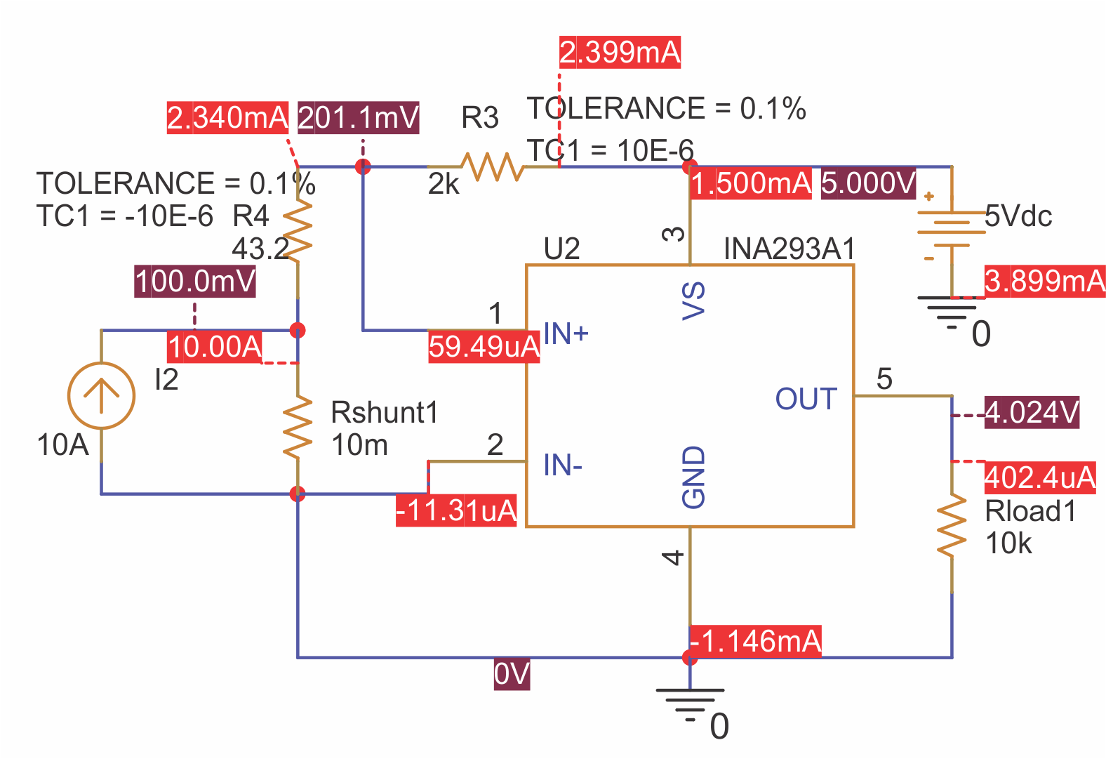
Error Calculations R1 MAX R2 MINError Calculations:
All cases are simulated: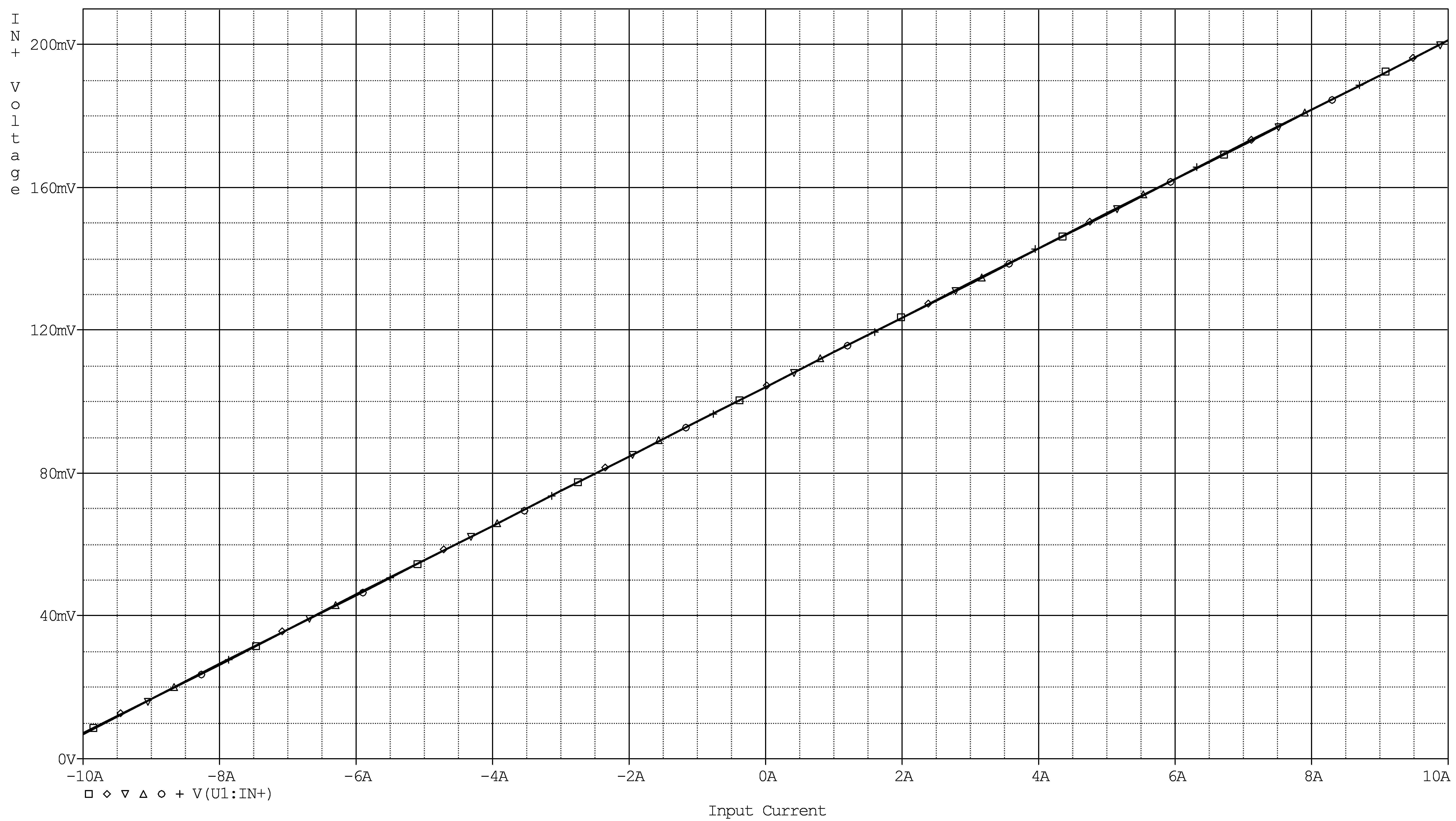
IN+ Voltage vs Input CurrentMeasurement TableMeasurements (mV) (1) (2) (3) (4) (5) (6) Max(V(U1:IN+)) 201.16 201.36 201.11 201.31 200.99 201.19 Min(V(U1:IN+)) 7.01 7.22 6.96 7.17 6.84 7.04 (1) Nominal Values at 0°C(2) Worst-Case Values at 0°C(3) Nominal Values at 27°C(4) Worst-Case Values at 27°C(5) Nominal Values at 85°C(6) Worst-Case Values at 85°C - R1min in
combination with R2max
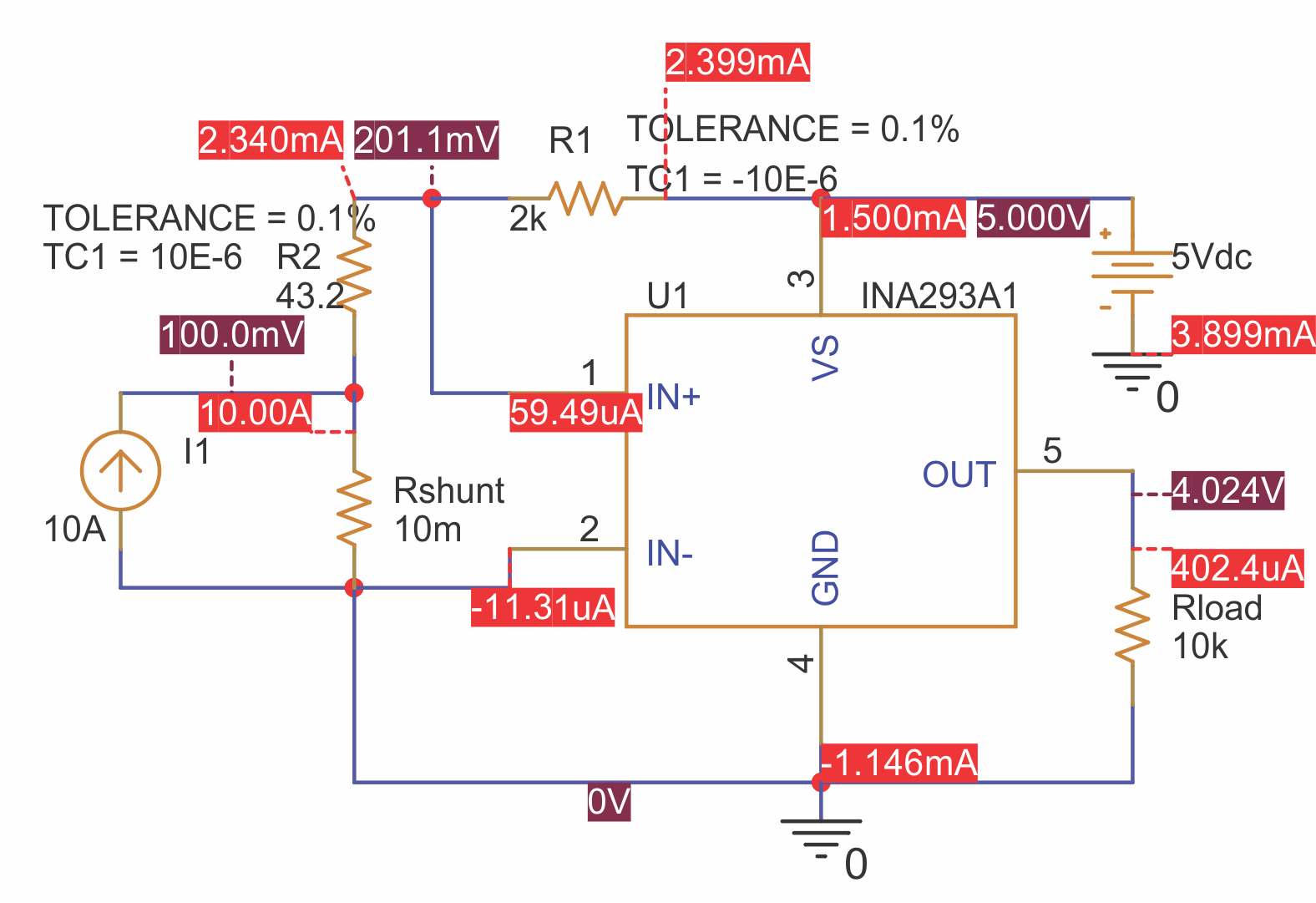
R1 MIN R2 MAXThe input-voltage vs. input-current plot looks almost the same as under R1max in combination with R2min.
Measurement TableMeasurements (mV) (1) (2) (3) (4) (5) (6) Max(V(U1:IN+)) 201.06 201.25 201.11 201.31 201.23 201.42 Min(V(U1:IN+)) 6.90 7.11 6.96 7.17 7.08 7.29 (1) Nominal Values at 0°C(2) Worst-Case Values at 0°C(3) Nominal Values at 27°C(4) Worst-Case Values at 27°C(5) Nominal Values at 85°C(6) Worst-Case Values at 85°C
Error at 27°C Room Temperature
Because the difference between the worst-case (column 4) and nominal (column 3) curve is constant, this results in an error caused by R1 and R2 at 27°C of
201.31 mV / 201.11 mV – 1 = 0.1% at +10 A
and
7.17 mV
/ 6.96 mV – 1 = 3% at –10 A.
Error Over Temperature Range
From the measurement tables, the minimum and maximum input voltages at IN+ are:
- –10 A: 6.84 mV and 7.29 mV, highlighted in green in the measurement tables
- +10 A: 200.99 mV and 201.42 mV, highlighted in blue in the measurement tables
| Input Current | Error at Room Temperature 27°C | Error from 0°C to 85°C |
|---|---|---|
| –10 A | +3% | +4.47% | –1.72% |
| +10 A | +0.1% | +0.15% | –0.06% |
Because the delta of the worst-case voltages at VIN stays constant over the whole current range, the error becomes smaller with higher input voltage.
VOUT can be calculated with VIN multiplied by 20, the gain of the INA293A1:
Vout,min = 6.84 mV × 20 = 137 mV and Vout,max = 201.42 mV × 20 = 4.03 V which meets the design goal.
Design References
See Analog Engineer's Circuit Cookbooks for TI's comprehensive circuit library.
Download the PSpice files for this circuit – www.ti.com/lit/zip/SBOA529.
For more information on the INA293 device, see the INA293 –4-V to 110-V, 1-MHz, High-Precision Current Sense Amplifier data sheet.
Additional Resources
- PSpice® for TI design and simulation tool: PSPICE-FOR-TI