SBOA545 March 2022 INA293
Design Goals
The design goal is the realization of a high-side, bidirectional current sensing circuit using a unidirectional current sense amplifier.
| Input | Output | Supply | Error | ||
|---|---|---|---|---|---|
| IMin | IMax | Vout, min | Vout, max | VS | Output Error |
| –10 A | +10 A | 50 mV | 4.8 V | 5 V | ≤ 2% |
Design Description
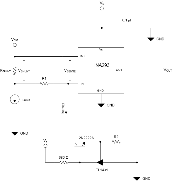
This circuit utilizes a TL1431, 2N2222A NPN transistor (see the following image), and passive components to achieve bidirectional sensing from a unidirectional current sense amplifier, the INA293. In this particular setup, the normal operating load is from –10 A to 10 A, with a supply voltage of 5 V. This topology may be used for any supply voltage independent of the desired offset. The solution presented in this circuit is a high-side implementation, with a common-mode voltage range of 2.5 V to 110 V.
 INA293 High-Side Bidirectional Schematic
Design Notes
- This topology is meant for
high-side implementation, where the IN+ and IN– pin of the INA293 are referenced
to the common-mode voltage (VCM) of the application. While this
circuit is capable of withstanding the full 110-V common mode of the INA293, a
limitation exists on the lower end, and VCM must be held
> 2.5 V. This is due to reference of the TL1431 of 2.5 V, and the need for the current flow to sink towards the TL1431 for proper offset voltage creation. Therefore, the common-mode voltage of the IN– pin must be
> 2.5 V to ensure valid operation. - For the presented design, a 24
VCM is considered, and the 2N2222A is chosen to complete the
design based on these parameters. A BJT possessing greater VCE
capabilities is needed for high-voltage applications
> 50 VCM. - While this circuit provides the ability to measure in multiple directions, it does not change the fact that the INA293 is inherently a unidirectional device. This infers that one direction of current sensing will be more accurate than the other, as one direction will measure towards the offset voltage of the device, leading to increased error in this direction. The effects of this may be mitigated in part by the use of a one-point calibration, and is discussed later in this document.
Design Steps
- Design the Offset Current: The offset current ultimately flows over R1 to create the referred to input (RTI) offset sense voltage, and is determined by resistor R2. The default reference voltage of the TL1431 is 2.5 V, and here, a 1-kΩ resistor is chosen, and the offset current is calculated as shown in the following equation:
- Design RTI Offset Voltage Point: With IOFFSET determined in the previous equation, R1 may now be selected to determine the reference point of the design (VREF). This point needs to be chosen based on where the origin of the output to be located is wanted. This is typically influenced by swing-to-rail limitations, as well as the defined linear operating region for the device in question. From the gain error specification of the INA293, the linear operating region is defined as from 50 mV above GND, to 200 mV below supply, and this is chosen to be the limiting bounds of the design to maximize accuracy. For these points, a roughly equidistant VREF of 2.4 V was chosen, but actual resistor selection of R1 (48.7 Ω from the ideal 48 Ω) ultimately led to a 2.435-V design. This point is determined by the following equations:
- Choose RSHUNT to Optimize Input Range: With the RTI Offset designed, a shunt may now be chosen for the desired sensing range, taking the constant RTI offset voltage into account. For the desired lower bound of 50 mV, this correlates to a 2.5-mV sense voltage referred to the input pins of the INA293, while the upper bound correlates to 240 mV. From the desired bound design targets, for the A1 variant, it is calculated that the maximum allowable shunt to achieve this goal is found using the following:
Using the lesser of these values, this shows that a maximum 11.825-mΩ shunt may be used to satisfy the upper bound, and some small truncation of the lower region should be expected. Choosing a convenient standard value resistor, 10 mΩ was selected to complete the design. The final input VSENSE swing is calculated as:
The expected corresponding output is found using:
The designed outputs are found to be within the linear operating range, but fall short of utilizing the full dynamic range here. The reason for this is due to the choice of sense resistor of 10 mΩ versus the defined maximum of 11.8 mΩ. Range may be increased further, but this will often come at the tradeoff of increased BOM cost for custom values, or additional components to form parallel combinations that achieve a closer target to the theoretical maximum.
- Verify shunt derating is sufficient: A necessary aspect of proper shunt design is ensuring that the design choice has sufficient margin for power derating. As the device heats in the environment, the amount of power the shunt is capable of dissipating is derated by a certain factor. For continuous sensing, this factor can be as high as 0.6. Taking this into account, for the design, a shunt must be chosen that is rated for at least the following:
So for a successful design, a shunt of at least 2 W rated power is chosen for continuous sensing.
- Choose the correct BJT NPN transistor: Dependent on the common modes expected to be seen by the application, a corresponding BJT must be chosen to be able to withstand this VCM. The voltage ultimately seen by the BJT is calculated as in the following equation:
Add some margin for any potential voltage transients on the common mode. For the given design, the 2N2222A is chosen, as it is able to withstand a VCE of 50 V maximum, and meets the needs of the design. The expected power dissipated through the BJT is found with the following equation:
- Examine Error. Calibrate if necessary: As discussed in previous sections, it is expected that the current sense amplifier will be more accurate in the direction of measurement as the output is driven toward supply. Less accurate measurements are expected as the sense voltage decreases, and errors from the offset voltage begin to have more effect. A remedy for this is to perform a one-point calibration in logic to reduce the effects of the offset voltage, if necessary. Here, the design is within the design goal, so this is not necessary.
Design Simulations and Calculations
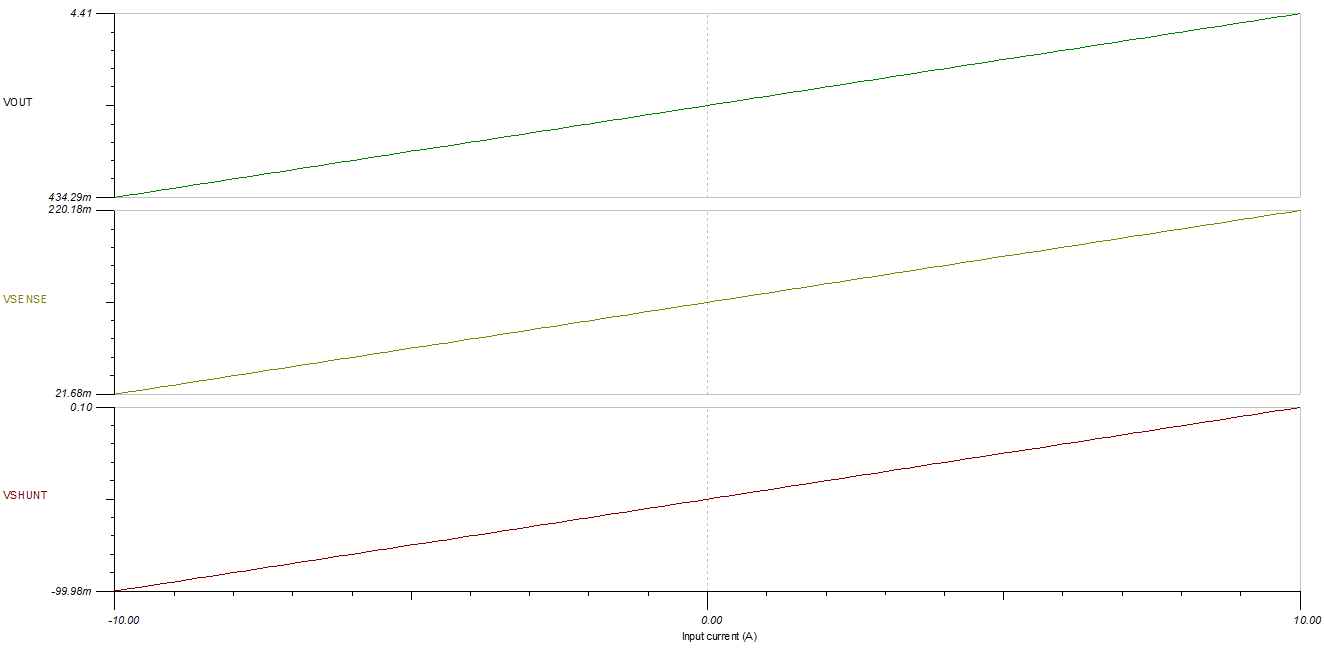
DC Sweep Results, –10 A < ILOAD < 10 A
 DC Load Current Sweep, Sense Voltage, and Output
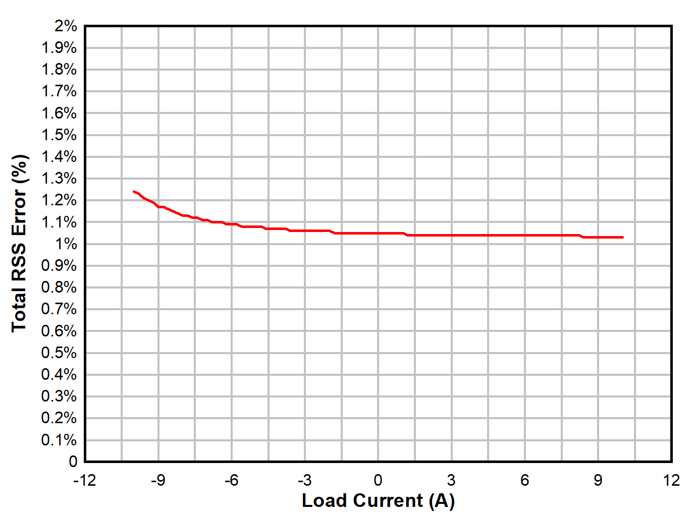
The following Root-Sum-Square (RSS) error curve was generated for the following resistor tolerances and RSS equation:
- RSHUNT = ±0.1%
- R1 = ±1%
- R2 = ±1%
Note that more accurate resistors will result in further reduction of the total error curve.
 INA293 Bidirectional Circuit RSS Maximum Error Curve
Design References
See Analog Engineer's Circuit Cookbooks for TI's comprehensive circuit library.
Download the PSpice files for this circuit – SBOA545.
For more information on the INA293 device, see the INA293 –4-V to 110-V, 1-MHz, High-Precision Current Sense Amplifier data sheet.
Additional Resources
- PSpice® for TI design and simulation tool: PSPICE-FOR-TI