SBVS080J September 2006 – November 2016 TPS75100 , TPS75103 , TPS75105
PRODUCTION DATA.
- 1 Features
- 2 Applications
- 3 Description
- 4 Revision History
- 5 Pin Configuration and Functions
- 6 Specifications
- 7 Detailed Description
- 8 Application and Implementation
- 9 Power Supply Recommendations
- 10Layout
- 11Device and Documentation Support
- 12Mechanical, Packaging, and Orderable Information
1 Features
- Regulated Output Current with 2% LED-to-LED Matching
- Drives Up to Four LEDs at 25 mA Each in a Common Cathode Topology
- 28-mV Typical Dropout Voltage Extends Usable Supply Range in Li-Ion Battery Applications
- Brightness Control Using PWM Signals
- Two 2-LED Banks With Independent Enable and PWM Brightness Control per Bank
- No Internal Switching Signals—Eliminates EMI
- Default LED Current Eliminates External Components
- Default Values from 3 mA to 10 mA (in 1-mA Increments) Available Using Innovative Factory EEPROM Programming
- Optional External Resistor can be Used for High-Accuracy, User-Programmable Current
- Over current and Over temperature Protection
- Available in Wafer Chip-Scale Package
or 2.50-mm × 2.50-mm WSON-10
2 Applications
- Keypad and Display Backlighting
- White and Color LEDs
- Cellular Handsets
- PDAs and Smartphones
3 Description
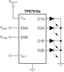
The TPS7510x linear low dropout (LDO) matching LED current source is optimized for low-power keypad and navigation pad LED backlighting applications. The device provides a constant current to up to four unmatched LEDs organized in two banks of two LEDs each in a common-cathode topology. Without an external resistor, the current source defaults to a factory-programmable, preset current level with ±0.5% accuracy (typical). An optional external resistor can be used to set initial brightness to user-programmable values with higher accuracy. Brightness can be varied from off to full brightness by inputting a pulse width modulation (PWM) signal on each enable pin (ENx, where x indicates LED bank A or B). Each bank has independent enable and brightness control, but current matching is done to all four channels concurrently. The input supply range is ideally suited for single-cell Li-Ion battery supplies and the TPS7510x can provide up to 25 mA per LED.
No internal switching signals are used, eliminating troublesome electromagnetic interference (EMI). The TPS7510x is offered in an ultra-small, 9-ball, 0.4-mm ball-pitch wafer chip-scale package (WCSP) and a 2.50-mm × 2.50-mm, 10-pin WSON package, yielding a very compact total solution size ideal for mobile handsets and portable backlighting applications. The device is fully specified over TJ = –40°C to +85°C.
Device Information(1)
| PART NUMBER | PACKAGE | BODY SIZE (NOM) |
|---|---|---|
| TPS7510x | WSON (10) | 2.50 mm × 2.50 mm |
| DSBGA (9) | 1.208 mm x 1.208 mm |
- For all available packages, see the orderable addendum at the end of the data sheet.
