SNVS528H October 2007 – January 2016 LM20143 , LM20143-Q1
PRODUCTION DATA.
- 1 Features
- 2 Applications
- 3 Description
- 4 Revision History
- 5 Pin Configuration and Functions
- 6 Specifications
- 7 Detailed Description
-
8 Application and Implementation
- 8.1 Application Information
- 8.2
Typical Applications
- 8.2.1
3.3-V or 5-V Supply Rail Design
- 8.2.1.1 Design Requirements
- 8.2.1.2
Detailed Design Procedure
- 8.2.1.2.1 Duty Cycle Calculation
- 8.2.1.2.2 Inductor Selection (L)
- 8.2.1.2.3 Output Capacitor Selection (COUT)
- 8.2.1.2.4 Input Capacitor Selection (CIN)
- 8.2.1.2.5 Setting the Output Voltage (RFB1, RFB2)
- 8.2.1.2.6 Adjusting the Operating Frequency (RT)
- 8.2.1.2.7 AVIN Filtering Components (CF and RF)
- 8.2.1.2.8 Sub-Regulator Bypass Capacitor (CVCC)
- 8.2.1.2.9 Setting the Start Up Time (CSS)
- 8.2.1.2.10 Loop Compensation (RC1, CC1)
- 8.2.1.3 Application Curves
- 8.2.2 5-V Supply Rail Design
- 8.2.3 3-V Supply Rail Design
- 8.2.1
3.3-V or 5-V Supply Rail Design
- 9 Power Supply Recommendations
- 10Layout
- 11Device and Documentation Support
- 12Mechanical, Packaging, and Orderable Information
Package Options
Mechanical Data (Package|Pins)
- PWP|16
Thermal pad, mechanical data (Package|Pins)
- PWP|16
Orderable Information
1 Features
- Available in AEC-Q100 Temperature Grade 1
- Input Voltage Range: 2.95 V to 5.50 V
- Accurate Current Limit Minimizes Inductor Size
- 97% Peak Efficiency
- Adjustable Output Voltage Down to 0.80 V
- Adjustable Switching Frequency (500 kHz to 1.5 MHz)
- 32-mΩ Integrated FET Switches
- Starts into Prebiased Loads
- Output Voltage Tracking
- Peak Current Mode Control
- Adjustable Soft-Start with External Capacitor
- Precision Enable Pin with Hysteresis
- Integrated OVP, UVLO, Power Good and Thermal Shutdown
2 Applications
- Simple to Design, High Efficiency Point of Load Regulation from a 5-V or 3.3-V Bus
- High Performance DSPs, FPGAs, ASICs, and Microprocessors
- Broadband, Networking, and Optical Communications Infrastructure
3 Description
The LM20143 devices are full featured PowerWise™ adjustable frequency synchronous buck regulators capable of delivering up to 3 A of continuous output current. The current mode control loop can be compensated to be stable with virtually any type of output capacitor. For most cases, compensating the device only requires two external components, providing maximum flexibility and ease of use. The device is optimized to work over the input voltage range of 2.95 V to 5.5 V, making it suited for a wide variety of low voltage systems.
The device features internal over voltage protection (OVP) and over current protection (OCP) circuits for increased system reliability. A precision enable pin and integrated UVLO allows the turn-on of the device to be tightly controlled and sequenced. Start-up inrush currents are limited by both an internally fixed and externally adjustable Soft-Start circuit. Fault detection and supply sequencing is possible with the integrated power good circuit.
The frequency of this device can be adjusted from 500 kHz to 1.5 MHz by connecting an external resistor from the RT pin to ground.
The LM20143 is designed to work well in multi-rail power supply architectures. The output voltage of the device can be configured to track a higher voltage rail using the SS/TRK pin. If the output of the LM20143 is pre-biased at startup it will not sink current to pull the output low until the internal soft-start ramp exceeds the voltage at the feedback pin.
Device Information(1)
| PART NUMBER | PACKAGE | BODY SIZE (NOM) |
|---|---|---|
| LM20143 | HTSSOP (16) | 4.40 mm × 5.00 mm |
| LM20143-Q1 |
- For all available packages, see the orderable addendum at the end of the data sheet.
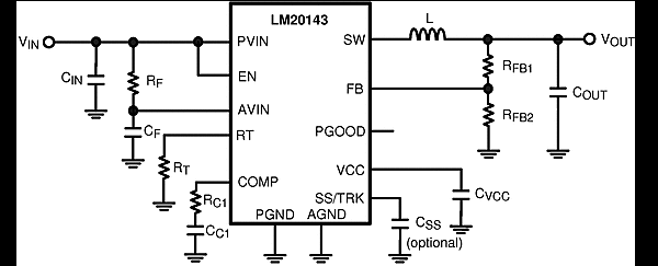
Typical Application Circuit
