SLCS007K September 1973 – March 2017 LM111 , LM211 , LM311
PRODUCTION DATA.
- 1 Features
- 2 Applications
- 3 Description
- 4 Revision History
- 5 Pin Configuration and Functions
- 6 Specifications
- 7 Parameter Measurement Information
- 8 Detailed Description
- 9 Application and Implementation
- 10Power Supply Recommendations
- 11Layout
- 12Device and Documentation Support
- 13Mechanical, Packaging, and Orderable Information
Package Options
Refer to the PDF data sheet for device specific package drawings
Mechanical Data (Package|Pins)
- D|8
- P|8
- PW|8
Thermal pad, mechanical data (Package|Pins)
Orderable Information
1 Features
- Fast Response Time: 165 ns
- Strobe Capability
- Maximum Input Bias Current: 300 nA
- Maximum Input Offset Current: 70 nA
- Can Operate From Single 5-V Supply
- Available in Q-Temp Automotive
- High-Reliability Automotive Applications
- Configuration Control and Print Support
- Qualification to Automotive Standards
-
On Products Compliant to MIL-PRF-38535,
All Parameters Are Tested Unless Otherwise Noted. On All Other Products, Production Processing Does Not Necessarily Include Testing of All Parameters.
2 Applications
3 Description
The LM111, LM211, and LM311 devices are single high-speed voltage comparators. These devices are designed to operate from a wide range of power-supply voltages, including ±15-V supplies for operational amplifiers and 5-V supplies for logic systems. The output levels are compatible with most TTL and MOS circuits. These comparators are capable of driving lamps or relays and switching voltages up to 50 V at 50 mA. All inputs and outputs can be isolated from system ground. The outputs can drive loads referenced to ground, VCC+ or VCC−. Offset balancing and strobe capabilities are available, and the outputs can be wire-OR connected. If the strobe is low, the output is in the off state, regardless of the differential input.
Device Information(1)
| PART NUMBER | PACKAGE | BODY SIZE |
|---|---|---|
| LM111FK | LCCC (20) | 8.89 mm × 8.89 mm |
| LM111JG | CDIP (8) | 9.60 mm × 6.67 mm |
| LM311PS | SO (8) | 6.20 mm × 5.30 mm |
| LM211D | SOIC (8) | 4.90 mm × 3.91 mm |
| LM311D | ||
| LM211P | PDIP (8) | 9.81 mm × 6.35 mm |
| LM311P | ||
| LM211PW | TSSOP (8) | 3.00 mm × 4.40 mm |
| LM311PW |
- For all available packages, see the orderable addendum at the end of the data sheet.
SPACER
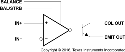
Simplified Schematic
