SNVSAR4A December 2016 – April 2017 LMR23610-Q1
PRODUCTION DATA.
- 1 Features
- 2 Applications
- 3 Description
- 4 Revision History
- 5 Pin Configuration and Functions
- 6 Specifications
-
7 Detailed Description
- 7.1 Overview
- 7.2 Functional Block Diagram
- 7.3
Feature Description
- 7.3.1 Fixed Frequency Peak Current Mode Control
- 7.3.2 Adjustable Output Voltage
- 7.3.3 Enable/Sync
- 7.3.4 VCC, UVLO
- 7.3.5 Minimum ON-time, Minimum OFF-time and Frequency Foldback at Drop-out Conditions
- 7.3.6 Internal Compensation and CFF
- 7.3.7 Bootstrap Voltage (BOOT)
- 7.3.8 Over Current and Short Circuit Protection
- 7.3.9 Thermal Shutdown
- 7.4 Device Functional Modes
-
8 Application and Implementation
- 8.1 Application Information
- 8.2
Typical Applications
- 8.2.1 Design Requirements
- 8.2.2
Detailed Design Procedure
- 8.2.2.1 Custom Design With WEBENCH® Tools
- 8.2.2.2 Output Voltage Set-Point
- 8.2.2.3 Switching Frequency
- 8.2.2.4 Inductor Selection
- 8.2.2.5 Output Capacitor Selection
- 8.2.2.6 Feed-Forward Capacitor
- 8.2.2.7 Input Capacitor Selection
- 8.2.2.8 Bootstrap Capacitor Selection
- 8.2.2.9 VCC Capacitor Selection
- 8.2.2.10 Under Voltage Lockout Set-Point
- 8.2.3 Application Curves
- 9 Power Supply Recommendations
- 10Layout
- 11Device and Documentation Support
- 12Mechanical, Packaging, and Orderable Information
Package Options
Refer to the PDF data sheet for device specific package drawings
Mechanical Data (Package|Pins)
- DDA|8
Thermal pad, mechanical data (Package|Pins)
- DDA|8
Orderable Information
1 Features
- Qualified for Automotive Applications
- AEC-Q100 Qualified With the Following Results:
- Device Temperature Grade 1: -40 °C to 125 °C Ambient Operating Temperature Range
- Device HBM ESD Classification Level H1C
- Device CDM ESD Classification Level C4A - 4 V to 36 V Input Range
- 1 A Continuous Output Current
- Integrated Synchronous Rectification
- Current Mode Control
- Minimum Switch-On Time: 60 ns
- Internal Compensation for Ease of Use
- 400 kHz Switching Frequency With PFM Mode
- Frequency Synchronization to External Clock
- 75 µA Quiescent Current at No Load
- Soft-Start into a Pre-Biased Load
- High Duty Cycle Operation Supported
- Output Short-Circuit Protection with Hiccup Mode
- 8-Pin HSOIC with PowerPAD™ Package Options
- Create a Custom Design Using the LMR23610-Q1 With the WEBENCH® Power Designer
2 Applications
- Automotive Battery Regulation
- Industrial Power Supplies
- Telecom and Datacom Systems
- General Purpose Wide Vin Regulation
space
3 Description
The LMR23610-Q1 SIMPLE SWITCHER® is an easy to use 36 V, 1 A synchronous step down regulator. With a wide input range from 4 V to 36 V, it is suitable for various applications from industrial to automotive for power conditioning from unregulated sources. Peak current mode control is employed to achieve simple control loop compensation and cycle-by-cycle current limiting. A quiescent current of 75 µA makes it suitable for battery powered systems. Internal loop compensation means that the user is free from the tedious task of loop compensation design. This also minimizes the external components. An extended family is available in 1.5 A (LMR23615-Q1), 2.5 A (LMR23625-Q1) and 3 A (LMR23630-Q1) load current options in pin-to-pin compatible packages which allows simple, optimum PCB layout. A precision enable input allows simplification of regulator control and system power sequencing. Protection features include cycle-by-cycle current limit, hiccup mode short circuit protection and thermal shutdown due to excessive power dissipation.
Device Information(1)
| PART NUMBER | PACKAGE | BODY SIZE (NOM) |
|---|---|---|
| LMR23610AQDDARQ1 | HSOIC (8) | 4.9 mm x 3.9 mm |
- For all available packages, see the orderable addendum at the end of the data sheet.
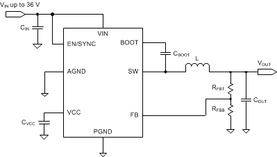
Simplified Schematic

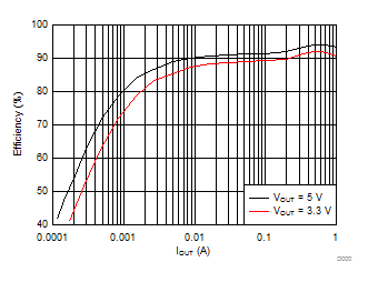
Efficiency vs Load, VIN = 12 V
