SLAS834C November 2012 – December 2014 RF430FRL152H , RF430FRL153H , RF430FRL154H
PRODUCTION DATA.
- 1Device Overview
- 2Revision History
- 3Device Comparison
- 4Terminal Configuration and Functions
-
5Specifications
- 5.1 Absolute Maximum Ratings
- 5.2 ESD Ratings
- 5.3 Recommended Operating Conditions
- 5.4 Recommended Operating Conditions, Resonant Circuit
- 5.5 Active Mode Supply Current Into VDDB Excluding External Current
- 5.6 Low-Power Mode Supply Current (Into VDDB) Excluding External Current
- 5.7 Digital I/Os (P1, RST/NMI)
- 5.8 High-Frequency Oscillator (4 MHz), HFOSC
- 5.9 Low-Frequency Oscillator (256 kHz), LFOSC
- 5.10 Wake-Up From Low-Power Modes
- 5.11 Timer_A
- 5.12 eUSCI (SPI Master Mode) Recommended Operating Conditions
- 5.13 eUSCI (SPI Master Mode)
- 5.14 eUSCI (SPI Slave Mode)
- 5.15 eUSCI (I2C Mode)
- 5.16 FRAM
- 5.17 JTAG
- 5.18 RFPMM, Power Supply Switch
- 5.19 RFPMM, Bandgap Reference
- 5.20 RFPMM, Voltage Doubler
- 5.21 RFPMM, Voltage Supervision
- 5.22 SD14, Performance
- 5.23 SVSS Generator
- 5.24 Thermistor Bias Generator
- 5.25 Temperature Sensor
- 5.26 RF13M, Power Supply and Recommended Operating Conditions
- 5.27 RF13M, ISO/IEC 15693 ASK Demodulator
- 5.28 RF13M, ISO/IEC 15693 Compliant Load Modulator
-
6Detailed Description
- 6.1 CPU
- 6.2 Instruction Set
- 6.3 Operating Modes
- 6.4 Interrupt Vector Addresses
- 6.5 Memory
- 6.6
Peripherals
- 6.6.1 Digital I/O, (P1.x)
- 6.6.2 Versatile I/O Port P1
- 6.6.3 Oscillator and System Clock
- 6.6.4 Compact System Module (C-SYS_A)
- 6.6.5 Watchdog Timer (WDT_A)
- 6.6.6 Reset, NMI, SVMOUT System
- 6.6.7 Timer_A (Timer0_A3)
- 6.6.8 Enhanced Universal Serial Communication Interface (eUSCI_B0)
- 6.6.9 ISO/IEC 15693 Analog Front End (RF13M)
- 6.6.10 ISO/IEC 15693 Decoder/Encoder (RF13M)
- 6.6.11 CRC16 Module (CRC16)
- 6.6.12 14-Bit Sigma-Delta ADC (SD14)
- 6.6.13 Programmable Gain Amplifier (SD14)
- 6.6.14 Peripheral Register Map
- 6.7 Port Schematics
- 6.8 Device Descriptors (TLV)
- 7Applications, Implementation, and Layout
- 8Device and Documentation Support
- 9Mechanical Packaging and Orderable Information
Package Options
Mechanical Data (Package|Pins)
- RGE|24
Thermal pad, mechanical data (Package|Pins)
- RGE|24
Orderable Information
1 Device Overview
1.1 Features
- ISO/IEC 15693, ISO/IEC 18000-3 (Mode 1) Compliant RF Interface
- Power Supply System With Either Battery or 13.56-MHz H-Field Supply
- 14-Bit Sigma-Delta Analog-to-Digital Converter (ADC)
- Internal Temperature Sensor
- Resistive Sensor Bias Interface
- CRC16 CCITT Generator
- MSP430™ Mixed-Signal Microcontroller
- 2KB of FRAM
- 4KB of SRAM
- 8KB of ROM
- Supply Voltage Range: 1.45 V to 1.65 V
- Low Power Consumption
- Active Mode (AM): 140 µA/MHz (1.5 V)
- Standby Mode (LPM3): 16 µA
- 16-Bit RISC Architecture
- Up to 2-MHz CPU System Clock
- Compact Clock System
- 4-MHz High-Frequency Clock
- 256-kHz Internal Low-Frequency Clock Source
- External Clock Input
- 16-Bit Timer_A With Three Capture/Compare Registers
- LV Port Logic
- VOL Lower Than 0.15 V at 400 µA
- VOH Higher Than (VDDB – 0.15 V) at 400 µA
- Timer_A PWM Signal Available on All Ports
- eUSCI_B Module Supports 3-Wire and 4-Wire SPI and I2C
- 32-Bit Watchdog Timer (WDT_A)
- ROM Development Mode (Map ROM Addresses to SRAM to Enable Firmware Development)
- Full 4-Wire JTAG Debug Interface
- For Complete Module Descriptions, See the RF430FRL15xH Family Technical Reference Manual (SLAU506)
- For Application Operation and Programming, See the RF430FRL15xH Firmware User's Guide (SLAU603)
1.2 Applications
- Industrial Wireless Sensors
- Medical Wireless Sensors
1.3 Description
The RF430FRL15xH device is a 13.56-MHz transponder chip with a programmable 16-bit MSP430™ low-power microcontroller. The device features embedded universal FRAM nonvolatile memory for storage of program code or user data such as calibration and measurement data. The RF430FRL15xH supports communication, parameter setting, and configuration through the ISO/IEC 15693, ISO/IEC 18000-3 compliant RFID interface and the SPI or I2C interface. Sensor measurements are supported by the internal temperature sensor and the onboard 14-bit sigma-delta analog-to-digital converter (ADC), and digital sensors can be connected through SPI or I2C.
The RF430FRL15xH device is optimized for operation in fully passive (battery-less) or single-cell battery-powered (semi-active) mode to achieve extended battery life in portable and wireless sensing applications. FRAM is a nonvolatile memory that combines the speed, flexibility, and endurance of SRAM with the stability and reliability of flash, all at lower total power consumption.
Device Information(1)
| PART NUMBER | PACKAGE | BODY SIZE(2) |
|---|---|---|
| RF430FRL152H | VQFN (24) | 4 mm x 4 mm |
| RF430FRL153H | VQFN (24) | 4 mm x 4 mm |
| RF430FRL154H | VQFN (24) | 4 mm x 4 mm |
1.4 Functional Block Diagram
Figure 1-1 shows the block diagram of the RF430FRL15xH device.
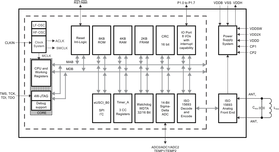 Figure 1-1 Functional Block Diagram