SLLSE15A July 2011 – November 2015 SN65LVDS4
PRODUCTION DATA.
- 1 Features
- 2 Applications
- 3 Description
- 4 Revision History
- 5 Pin Configuration and Functions
-
6 Specifications
- 6.1 Absolute Maximum Ratings
- 6.2 ESD Ratings
- 6.3 Recommended Operating Conditions
- 6.4 Thermal Information
- 6.5 Receiver Electrical Characteristics: VCC = 2.5 V
- 6.6 Receiver Electrical Characteristics: VCC = 1.8 V
- 6.7 Receiver Switching Characteristics: VCC = 2.5 V
- 6.8 Receiver Switching Characteristics: VCC = 1.8 V
- 6.9 Typical Characteristics
- 7 Parameter Measurement Information
- 8 Detailed Description
- 9 Application and Implementation
- 10Power Supply Recommendations
- 11Layout
- 12Device and Documentation Support
- 13Mechanical, Packaging, and Orderable Information
Package Options
Mechanical Data (Package|Pins)
- RSE|10
Thermal pad, mechanical data (Package|Pins)
Orderable Information
1 Features
- Designed for Signaling Rates up to: (1)
- Operates From a 1.8-V or 2.5-V Core Supply
- Available in 1.5-mm × 2-mm UQFN Package
- Bus-Terminal ESD Exceeds 2 kV (HBM)
- Low-Voltage Differential Signaling With Typical Output Voltages of 350 mV Into a 100-Ω Load
- Propagation Delay Times
- 2.1 ns Typical Receiver
- Power Dissipation at 250 MHz
- 40 mW Typical
- Requires External Failsafe
- Differential Input Voltage Threshold Less Than 50 mV
- Can Provide Output Voltage Logic Level (3.3-V LVTTL, 2.5-V LVCMOS, 1.8-V LVCMOS) Based on External VDD Pin, Thus Eliminating External Level Translation
(1) The signaling rate of a line is the number of voltage transitions that are made per second expressed in the units bps (bits per second)
2 Applications
- Clock Distribution
- Wireless Base Stations
- Network Routers
3 Description
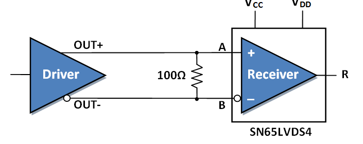
The SN65LVDS4 is a single, low-voltage, differential line receiver in a small-outline UQFN package.
Device Information(1)
| PART NUMBER | PACKAGE | BODY SIZE (NOM) |
|---|---|---|
| SN65LVDS4 | UQFN (10) | 1.50 mm × 2.00 mm |
- For all available packages, see the orderable addendum at the end of the datasheet.
Typical Application Circuits
