SLOS829A February 2013 – July 2015 THS4532
PRODUCTION DATA.
- 1 Features
- 2 Applications
- 3 Description
- 4 Revision History
- 5 Related Products
- 6 Pin Configuration and Functions
- 7 Specifications
- 8 Detailed Description
-
9 Application and Implementation
- 9.1
Application Information
- 9.1.1 Frequency Response and Output Impedance
- 9.1.2 Distortion
- 9.1.3 Slew Rate, Transient Response, Settling Time, Overdrive, Output Voltage, and Turnon and Turnoff Time
- 9.1.4 Common-Mode and Power Supply Rejection
- 9.1.5 VOCM Input
- 9.1.6 Balance Error
- 9.1.7 Single-Supply Operation
- 9.1.8 Low-Power Applications and the Effects of Resistor Values on Bandwidth
- 9.1.9 Driving Capacitive Loads
- 9.1.10 Audio Performance
- 9.1.11 Audio On and Off Pop Performance
- 9.2 Typical Applications
- 9.3 Systems Examples
- 9.1
Application Information
- 10Power Supply Recommendations
- 11Layout
- 12Device and Documentation Support
- 13Mechanical, Packaging, and Orderable Information
Package Options
Mechanical Data (Package|Pins)
- PW|16
Thermal pad, mechanical data (Package|Pins)
Orderable Information
1 Features
- Ultra Low Power:
- Voltage: 2.5 V to 5.5 V
- Current: 250 µA
- Power-Down Mode: 0.5 µA (typ)
- Fully-Differential Architecture
- Bandwidth: 36 MHz
- Slew Rate: 200 V/µs
- THD: –120 dBc at 1 kHz (1 VRMS, RL= 2 kΩ)
- Input Voltage Noise: 10 nV/√Hz (f = 1 kHz)
- High DC Accuracy:
- VOS: ±100 µV
- VOS Drift: ±3 µV/˚C (–40°C to +125°C)
- AOL: 114 dB
- Rail-to-Rail Output (RRO)
- Negative Rail Input (NRI)
- Output Common-Mode Control
2 Applications
- Low-Power SAR, ΔΣ ADC Driver
- Low Power, High Performance:
- Differential to Differential Amplifier
- Single-Ended to Differential Amplifier
- Low-Power, Wide-Bandwidth Differential Driver
- Low-Power, Wide-Bandwidth Differential Signal Conditioning
- High Channel Count and Power Dense Systems
3 Description
The THS4532 is a low-power, fully-differential amplifier with input common-mode range below the negative rail and rail-to-rail output. The device is designed for low-power data acquisition systems and high density applications where power consumption and dissipation is critical.
The device features accurate output common-mode control that allows for dc coupling when driving analog-to-digital converters (ADCs). This control, coupled with the input common-mode range below the negative rail and rail-to-rail output, allows for easy interface from single-ended ground-referenced signal sources to successive-approximation registers (SARs), and delta-sigma (ΔΣ) ADCs using only single-supply 2.5-V to 5-V power. The THS4532 is also a valuable tool for general-purpose, low-power differential signal conditioning applications.
The device is characterized for operation over the extended industrial temperature range from –40°C to 125°C. The following package options are available:
Device Information(1)
| PART NUMBER | PACKAGE | BODY SIZE (NOM) |
|---|---|---|
| THS4532 | TSSOP | 5.00 mm x 4.40 mm |
- For all available packages, see the orderable addendum at the end of the datasheet.
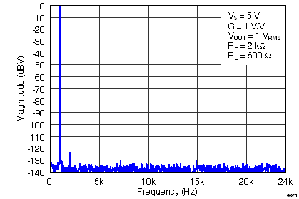
1-kHz FFT Plot on Audio Analyzer
