SLVS867B May 2009 – August 2015 TLC59213 , TLC59213A
PRODUCTION DATA.
- 1 Features
- 2 Applications
- 3 Description
- 4 Revision History
- 5 Pin Configuration and Functions
- 6 Specifications
- 7 Parameter Measurement Information
- 8 Detailed Description
- 9 Application and Implementation
- 10Power Supply Recommendations
- 11Layout
- 12Device and Documentation Support
- 13Mechanical, Packaging, and Orderable Information
Package Options
Mechanical Data (Package|Pins)
Thermal pad, mechanical data (Package|Pins)
Orderable Information
1 Features
- Output Current on Each Channel
(IOUT Max = –500 mA) - VCE(sus) = 13.2 V
- Input Compatible With TTL/5-V CMOS
- Clear (CLR) and Clock (CLK) TTL/CMOS Control Inputs
- CLR Control Input to Off the Output
- Darlington Source Driver
- Clock Input Up to 1 MHz
- Enhanced Hold Time (th) on TLC59213A
- Temperature Range: –40°C to 85°C
2 Applications
- Lamp and Display (LED)
- Hammer
- Relay
3 Description
The TLC59213 and TLC59213A are 8-bit source drivers with input latch with CLK input and CLR to set the output OFF. The TLC59213 and TLC59213A have large output source currents up to 500 mA with Darlington transistor and collectors tied to VCC. These feature make the device optimum level of driving the matrix of ink jet printer head, LEDs, and the scan-side of resistor's matrix. The TLC59213 and TLC59213A differ only in the Data Hold Time Specification (th).
The clamp diode is between output and ground for switching inductive load.
All inputs are TTL/CMOS, which enable to any logic-level inputs such as MCU, CPU or SN74LV594 (serial to parallel) and the output enable LED matrix display. It can also be used with another device sink driver such as TLC59210, TLC59211 and TLC59212.
Device Information(1)
| PART NUMBER | PACKAGE | BODY SIZE (NOM) |
|---|---|---|
| TLC59213 TLC59213A |
PDIP (20) | 24.33 mm × 6.35 mm |
| TSSOP (20) | 6.50 mm × 4.40 mm |
- For all available packages, see the orderable addendum at the end of the data sheet.
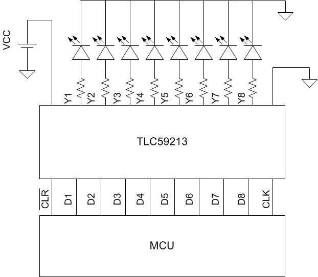
Typical Application Diagram÷
