SBOS783 September 2016 TLV171 , TLV2171 , TLV4171
PRODUCTION DATA.
- 1 Features
- 2 Applications
- 3 Description
- 4 Revision History
- 5 Pin Configuration and Functions
- 6 Specifications
- 7 Detailed Description
- 8 Application and Implementation
- 9 Power Supply Recommendations
- 10Layout
- 11Device and Documentation Support
- 12Mechanical, Packaging, and Orderable Information
Package Options
Mechanical Data (Package|Pins)
Thermal pad, mechanical data (Package|Pins)
Orderable Information
1 Features
- Supply Range: 2.7 V to 36 V, ±1.35 V to ±18 V
- Low Noise: 16 nV/√Hz
- Low Offset Drift: ±1 μV/°C (typical)
- EMI-Hardened with RFI-Filtered Inputs
- Input Range Includes the Negative Supply
- Unity-Gain Stable: 200-pF Capacitive Load
- Rail-to-Rail Output
- Gain Bandwidth: 3 MHz
- Low Quiescent Current: 525 µA per Amplifier
- High Common-Mode Rejection: 105 dB (typical)
- Low Bias Current: 10 pA
2 Applications
- Transducers
- Currency Counters
- AC-DC Converters
- Power Modules
- Inverters
- Test Equipment
- Battery-Powered Instruments
- TFT-LCD Drive Circuits
- Active Filters
3 Description
The 36-V TLVx171 family provides a low-power option for cost-conscious industrial and personal electronics systems requiring an electromagnetic interference (EMI)-hardened, low-noise, single-supply operational amplifier (op amp) that operates on supplies ranging from 2.7 V (±1.35 V) to 36 V (±18 V). The single-channel TLV171, dual-channel TLV2171, and quad-channel TLV4171 provide low offset, drift, quiescent current balanced with high bandwidth for the power. The devices are available in micropackages for space-constrained systems and feature identical specifications for maximum design flexibility.
Unlike most op amp, which are specified at only one supply voltage, the TLVx171 family is specified from 2.7 V to 36 V. Input signals beyond the supply rails do not cause phase reversal. The TLVx171 family is stable with capacitive loads up to 200 pF. The input can operate 100 mV below the negative rail and within 2 V of the top rail during normal operation. These devices can operate with a full rail-to-rail input 100 mV beyond the top rail, but with reduced performance within 2 V of the top rail.
The TLVx171 op amp family is specified from –40°C to +125°C.
Device Information(1)
| PART NUMBER | PACKAGE | BODY SIZE (NOM) |
|---|---|---|
| TLV171 | SOIC (8) | 4.90 mm × 3.91 mm |
| SOT-23 (5) | 2.90 mm × 1.60 mm | |
| TLV2171 | SOIC (8) | 4.90 mm × 3.91 mm |
| VSSOP (8) | 3.00 mm × 3.00 mm | |
| TLV4171 | SOIC (14) | 8.65 mm × 3.91 mm |
| TSSOP (14) | 5.00 mm × 4.40 mm |
- For all available packages, see the orderable addendum at the end of the data sheet.
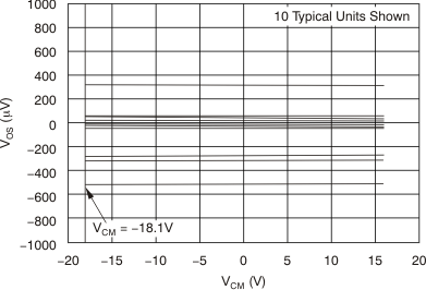
Offset Voltage vs Common-Mode Voltage

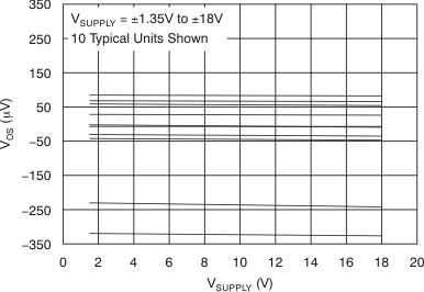
Offset Voltage vs Power Supply
