SLVSAK9H October 2011 – January 2017 TLV62080 , TLV62084 , TLV62084A
UNLESS OTHERWISE NOTED, this document contains PRODUCTION DATA.
- 1 Features
- 2 Applications
- 3 Description
- 4 Revision History
- 5 Device Comparison Table
- 6 Pin Configuration and Functions
- 7 Specifications
- 8 Detailed Description
- 9 Application and Implementation
- 10Power Supply Recommendations
- 11Layout
- 12Device and Documentation Support
- 13Mechanical, Packaging, and Orderable Information
Package Options
Mechanical Data (Package|Pins)
- DSG|8
Thermal pad, mechanical data (Package|Pins)
- DSG|8
Orderable Information
1 Features
- DCS-Control™ Architecture for Fast Transient Regulation
- 2.5 to 6-V Input Voltage Range (TLV62080)
- 2.7 to 6-V Input Voltage Range (TLV62084, TLV62084A)
- 100% Duty Cycle for Lowest Dropout
- Power Save Mode for Light Load Efficiency
- Output Discharge Function
- Power Good Output
- Thermal Shutdown
- Available in 2 mm × 2 mm 8-Terminal WSON Package
- For Improved Features Set, see the TPS62080
- Create a Custom Design Using the TLV6208x With the WEBENCH® Power Designer
2 Applications
3 Description
The TLV6208x family devices are small buck converters with few external components, enabling cost effective solutions. They are synchronous step-down converters with an input voltage range of 2.5 and 2.7 (2.5 V for TLV62080, 2.7 V for TLV62084x) to 6 V. The TLV6208x devices focus on high-efficiency step-down conversion over a wide output current range. At medium to heavy loads, the TLV6208x converters operate in PWM mode and automatically enter power save mode operation at light-load currents to maintain high efficiency over the entire load current range.
To address the requirements of system power rails, the internal compensation circuit allows a wide range of external output capacitor values. With the DCS-Control™ (Direct Control with Seamless transition into Power save mode) architecture excellent load transient performance and output voltage regulation accuracy are achieved. The devices are available in 2-mm × 2-mm WSON package with Thermal Pad.
Device Information(1)
| PART NUMBER | PACKAGE | BODY SIZE (NOM) |
|---|---|---|
| TLV62080 | WSON (8) | 2.00 mm × 2.00 mm |
| TLV62084, TLV62084A |
- For all available packages, see the orderable addendum at the end of the datasheet.
space
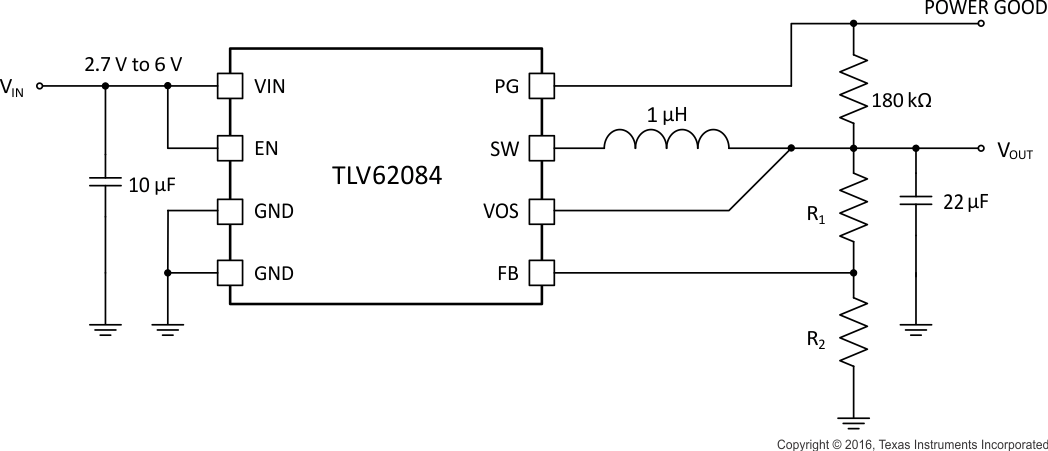
Typical Application Schematic |
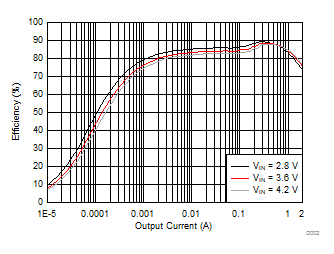
Efficiency vs Output Current, VOUT = 1.2V |
|
|
space |
space |
|
 |
 |
|