SBVS305 March 2017 TLV703
PRODUCTION DATA.
- 1 Features
- 2 Applications
- 3 Description
- 4 Revision History
- 5 Pin Configuration and Functions
- 6 Specifications
- 7 Detailed Description
- 8 Application and Implementation
- 9 Power Supply Recommendations
- 10Layout
- 11Device and Documentation Support
- 12Mechanical, Packaging, and Orderable Information
Package Options
Mechanical Data (Package|Pins)
- DBV|5
Thermal pad, mechanical data (Package|Pins)
Orderable Information
1 Features
- Very Low Dropout:
- 37 mV at IOUT = 50 mA, VOUT = 2.8 V
- 75 mV at IOUT = 100 mA, VOUT = 2.8 V
- 220 mV at IOUT = 300 mA, VOUT = 2.8 V
- 2% Accuracy
- Low IQ: 35 μA
- Fixed-Output Voltage Combinations Possible From 1.2 V to 4.8 V
- High PSRR: 68 dB at 1 kHz
- Stable With Effective Capacitance of 0.1 μF
- Thermal Shutdown and Overcurrent Protection
- Packages: 5-Pin SOT-23
2 Applications
- Wireless Handsets
- Smart Phones
- ZigBee® Networks
- Bluetooth® Devices
- Li-Ion Battery-Operated Handheld Products
- WLAN and Other PC Add-on Cards
3 Description
The TLV703 series of low-dropout (LDO) linear regulators are low quiescent current devices with excellent line and load transient performance. These LDOs are designed for power-sensitive applications. A precision band-gap and error amplifier provides overall 2% accuracy. Low output noise, very high power-supply rejection ratio (PSRR), and low-dropout voltage make this series of devices ideal for a wide selection of battery-operated handheld equipment. All device versions have thermal shutdown and current limit for safety.
Furthermore, these devices are stable with an effective output capacitance of only 0.1 µF. This feature enables the use of cost-effective capacitors that have higher bias voltages and temperature derating. The devices regulate to specified accuracy with no output load.
The TLV703 series of LDO linear regulators are available in a 5-pin SOT-23 package.
Device Information(1)
| PART NUMBER | PACKAGE | BODY SIZE (NOM) |
|---|---|---|
| TLV703 | SOT-23 (5) | 2.90 mm × 1.60 mm |
- For all available packages, see the orderable addendum at the end of the data sheet.
SPACE
SPACE
SPACE
SPACE
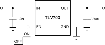
Typical Application Circuit
