SLVS749C November 2008 – January 2015 TPS22921 , TPS22922
UNLESS OTHERWISE NOTED, this document contains PRODUCTION DATA.
- 1 Features
- 2 Applications
- 3 Description
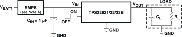
- 4 Typical Application
- 5 Revision History
- 6 Device Comparison Table
- 7 Pin Configuration and Functions
-
8 Specifications
- 8.1 Absolute Maximum Ratings
- 8.2 ESD Ratings
- 8.3 Recommended Operating Conditions
- 8.4 Thermal Information
- 8.5 Electrical Characteristics
- 8.6 Switching Characteristics: VIN = 0.9 V
- 8.7 Switching Characteristics: VIN = 1 V
- 8.8 Switching Characteristics: VIN = 1.1 V
- 8.9 Switching Characteristics: VIN = 1.2 V
- 8.10 Switching Characteristics: VIN = 1.8 V
- 8.11 Switching Characteristics: VIN = 2.5 V
- 8.12 Switching Characteristics: VIN = 3 V
- 8.13 Switching Characteristics: VIN = 3.6 V
- 8.14
Typical Characteristics
- 8.14.1 Typical DC Characteristics
- 8.14.2 Typical AC Characteristics (TPS22921)
- 8.14.3 Typical AC Characteristics (TPS22922)
- 8.14.4 Typical AC Characteristics (TPS22922B)
- 8.14.5 Typical AC Characteristics (TPS22921 and TPS22922)
- 8.14.6 Typical AC Characteristics (TPS22921)
- 8.14.7 Typical AC Characteristics (TPS22922)
- 8.14.8 Typical AC Characteristics (TPS22922B)
- 9 Parameter Measurement Information
- 10Detailed Description
- 11Application and Implementation
- 12Power Supply Recommendations
- 13Layout
- 14Device and Documentation Support
- 15Mechanical, Packaging, and Orderable Information
Package Options
Mechanical Data (Package|Pins)
Thermal pad, mechanical data (Package|Pins)
Orderable Information
1 Features
- Integrated P-Channel Load Switch
- Input Voltage: 0.9 V to 3.6 V
- ON-Resistance (Typical Values)
- rON = 14 mΩ at VIN = 3.6 V
- rON = 20 mΩ at VIN = 2.5 V
- rON = 33 mΩ at VIN = 1.8 V
- rON = 67 mΩ at VIN = 1.2 V
- rON = 116 mΩ at VIN = 1.0 V
- 2-A Maximum Continuous Switch Current
- Quiescent Current:
- Typical 78 nA at 1.8 V
- Shutdown Current:
- Typical 35 nA at 1.8 V
- Low Threshold Control Input Enable the use of
1.2 V, 1.8 V, 2.5 V, or 3.3 V Logic - Controlled Slew Rate to Avoid Inrush Currents
- tR = 30 μs at VIN = 1.8 V (TPS22921/2)
- tR = 200 μs at VIN = 1.8 V (TPS22922B)
- Quick Output Discharge (TPS22922/2B)
- ESD Performance Tested Per JESD 22
- 3000-V Human Body Model
(A114-B, Class II) - 1000-V Charged-Device Model (C101)
- 3000-V Human Body Model
- Six Terminal Wafer-Chip-Scale DSBGA Package (nominal dimensions shown - see Mechanical, Packaging, and Orderable Information for details)
2 Applications
- PDAs
- Cell Phones
- GPS Devices
- MP3 Players
- Peripheral Ports
- Portable Media Players
- RF Modules
3 Description
TPS22921, TPS22922, and TPS22922B are small, low rON load switches with controlled turnon. The TPS22921/2/2B contains a P-channel MOSFET that can operate over an input voltage range of 0.9 V to 3.6 V. The switch is controlled by an on/off input (ON), which can interface directly with low-voltage control signals. In TPS22922 and in TPS22922B, a 65-Ω on-chip load resistor is added for output quick discharge when the switch is turned off. The rise time (slew rate) of the device is internally controlled in order to avoid inrush current: TPS22921 and TPS22922 feature a 30-μs rise time, whereas TPS22922B is 200 μs.
TPS22921, TPS22922, and TPS22922B feature low quiescent and shutdown currents and are available in space-saving 6-pin wafer-chip-scale packages DSBGA (WCSP: YZP and YZT with 0.5-mm pitch and YFP with 0.4-mm pitch) which make them ideal for portable electronics. The devices are characterized for operation over the free-air temperature range of –40°C to 85°C.
Device Information(1)
| PART NUMBER | PACKAGE | BODY SIZE (NOM) |
|---|---|---|
| TPS22921(1) | YZT | 0.9 mm × 1.4 mm |
| YZP | ||
| YFP | 0.8 mm × 1.2 mm | |
| TPS22922 TPS22922B |
YZP | 0.9 mm × 1.4 mm |
| YFP | 0.8 mm × 1.2 mm |
- For all available packages, see the orderable addendum at the end of the data sheet.