SLVSCT5D March 2015 – September 2016 TPS22953 , TPS22954
PRODUCTION DATA.
- 1 Features
- 2 Applications
- 3 Description
- 4 Revision History
- 5 Device Comparison Table
- 6 Pin Configuration and Functions
-
7 Specifications
- 7.1 Absolute Maximum Ratings
- 7.2 ESD Ratings
- 7.3 Recommended Operating Conditions
- 7.4 Thermal Information
- 7.5 Electrical Characteristics
- 7.6 Electrical Characteristics—VBIAS = 5 V
- 7.7 Electrical Characteristics—VBIAS = 3.3 V
- 7.8 Electrical Characteristics—VBIAS = 2.5 V
- 7.9 Switching Characteristics—CT = 1000 pF
- 7.10 Switching Characteristics—CT = 0 pF
- 7.11 Typical DC Characteristics
- 7.12 Typical Switching Characteristics
- 8 Parameter Measurement Information
-
9 Detailed Description
- 9.1 Overview
- 9.2 Functional Block Diagram
- 9.3
Feature Description
- 9.3.1 On and Off Control (EN pin)
- 9.3.2 Voltage Monitoring (SNS Pin)
- 9.3.3 Power Good (PG Pin)
- 9.3.4 Supervisor Fault Detection and Automatic Restart
- 9.3.5 Manual Restart
- 9.3.6 Thermal Shutdown
- 9.3.7 Reverse Current Blocking (TPS22953 Only)
- 9.3.8 Quick Output Discharge (QOD) (TPS22954 Only)
- 9.3.9 VIN and VBIAS Voltage Range
- 9.3.10 Adjustable Rise Time (CT pin)
- 9.3.11 Power Sequencing
- 9.4 Device Functional Modes
- 10Application and Implementation
- 11Power Supply Recommendations
- 12Layout
- 13Device and Documentation Support
- 14Mechanical, Packaging, and Orderable Information
Package Options
Mechanical Data (Package|Pins)
Thermal pad, mechanical data (Package|Pins)
- DQC|10
Orderable Information
1 Features
- Integrated Single Channel Load Switch
- Input Voltage Range: 0.7 V to 5.7 V
- RON Resistance
- RON = 14 mΩ at VIN = 5 V (VBIAS = 5 V)
- 5-A Maximum Continuous Switch Current
- Adjustable Undervoltage Lockout Threshold (UVLO)
- Adjustable Voltage Supervisor with
Power Good (PG) Indicator - Adjustable Output Slew Rate Control
- Enhanced Quick Output Discharge Remains Active after Power is Removed (TPS22954 Only)
- 15 Ω (Typ) Discharges 100 µF Within 10 ms
- Reverse Current Blocking when Disabled (TPS22953 Only)
- Automatic Restart after Supervisor Fault Detection When Enabled
- Thermal Shutdown
- Low Quiescent Current ≤ 50 µA
- SON 10-pin Package with Thermal Pad
- ESD Performance Tested Per JESD 22
- 2-kV HBM and 750-V CDM
2 Applications
- Solid State Drives
- Embedded and Industrial PC
- Ultrabook™ and Notebooks
- Desktops
- Servers
- Telecom Systems
3 Description
The TPS22953/54 are small, single channel load switches with controlled turn on. The devices contain a N-channel MOSFET that can operate over an input voltage range of 0.7 V to 5.7 V and can support a maximum continuous current of 5 A.
The integrated adjustable undervoltage lockout (UVLO) and adjustable power good (PG) threshold provides voltage monitoring as well as robust power sequencing. The adjustable rise time control of the device greatly reduces inrush current for a wide variety of bulk load capacitances, thereby reducing or eliminating power supply droop. The switch is independently controlled by an on and off input (EN), which is capable of interfacing directly with low-voltage control signals. A 15-Ω on-chip load is integrated into the device for a quick discharge of the output when switch is disabled. The enhanced Quick Output Discharge (QOD) remains active for short time after power is removed from the device to finish discharging the output.
The TPS22953/54 are available in small, space-saving 10-SON packages with integrated thermal pad allowing for high power dissipation. The device is characterized for operation over the free-air temperature range of –40°C to +105°C.
Device Information(1)
| PART NUMBER | PACKAGE (PIN) | BODY SIZE (NOM) |
|---|---|---|
| TPS2295x | WSON (10) | 2.00 mm x 2.00 mm |
| WSON (10) | 2.00 mm x 3.00 mm |
- For all available packages, see the orderable addendum at the end of the datasheet.
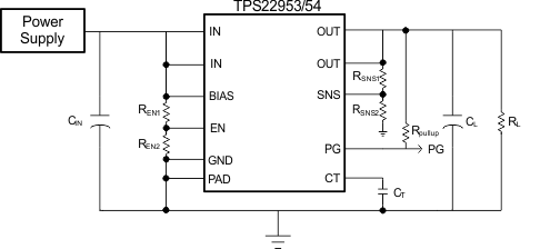
Simplified Schematic
