SLVSCQ8A December 2015 – April 2016 TPS54A20
PRODUCTION DATA.
- 1 Features
- 2 Applications
- 3 Description
- 4 Revision History
- 5 Pin Configuration and Functions
- 6 Specifications
-
7 Detailed Description
- 7.1 Overview
- 7.2 Functional Block Diagram
- 7.3
Feature Description
- 7.3.1 Frequency Selection
- 7.3.2 External Clock Syncronization
- 7.3.3 Adjusting the Output Voltage
- 7.3.4 Soft Start
- 7.3.5 Startup into Pre-biased Outputs
- 7.3.6 Power Good (PGOOD)
- 7.3.7 Overcurrent Protection
- 7.3.8 Light Load Operation
- 7.3.9 Output Undervoltage/Overvoltage Protection
- 7.3.10 Input Undervoltage/Overvoltage Lockout
- 7.3.11 Enable and Adjusting Undervoltage Lockout
- 7.3.12 Series Capacitor Monitoring
- 7.3.13 Thermal Shutdown
- 7.3.14 Phase A Power Stage
- 7.3.15 Phase B Power Stage
- 7.3.16 Internal Gate Drive Regulator
- 7.3.17 Voltage Feed Forward
- 7.3.18 Internal Oscillator
- 7.3.19 Pulse Frequency Detector
- 7.3.20 On-Time Generator
-
8 Application and Implementation
- 8.1 Application Information
- 8.2
Typical Application
- 8.2.1 Design Requirements
- 8.2.2
Detailed Design Procedure
- 8.2.2.1 Output Voltage
- 8.2.2.2 Switching Frequency
- 8.2.2.3 On-Time
- 8.2.2.4 Inductor Selection
- 8.2.2.5 Output Capacitor Selection
- 8.2.2.6 Input Capacitor Selection
- 8.2.2.7 Series Capacitor Selection
- 8.2.2.8 Soft-Start Time Selection
- 8.2.2.9 Bootstrap Capacitor Selection
- 8.2.2.10 Gate Drive Capacitor Selection
- 8.2.2.11 Under Voltage Lockout Set Point
- 8.2.2.12 Current Limit Selection
- 8.2.3 Application Curves
- 9 Power Supply Recommendations
- 10Layout
- 11Device and Documentation Support
- 12Mechanical, Packaging, and Orderable Information
Package Options
Refer to the PDF data sheet for device specific package drawings
Mechanical Data (Package|Pins)
- RNJ|20
Thermal pad, mechanical data (Package|Pins)
Orderable Information
1 Features
- Two-phase, Synchronous Series Capacitor Buck Converter
- Automatic Current Balancing Between Phases
- 2-MHz to 5-MHz Per Phase Switching Frequency
- 14-ns Minimum On-Time
- 0.51-V to 2-V Output Voltage Range with ±0.5% Feedback Reference Voltage
- Input Overvoltage Lockout for 17-V Surge Protection
- Adjustable Current Limit with Auto Restart (Hiccup)
- Synchronizes to an External Clock
- Fixed Frequency in Steady State
- Adaptive On-Time Control
- Internal Feedback Loop Compensation
- Internal Gate Drive LDO with External Supply Option
- EN Pin Allowing for Adjustable Input UVLO
- Selectable Soft-Start Time
- Monotonic Startup with Pre-biased Output
- Output Power Good Indicator (Open Drain)
- Output Overvoltage/Undervoltage Protection
2 Applications
- Telecom, base station, and communications equipment
- Storage, SSD, DDR memory, switches, hubs, routers, and other networking equipment
- Low profile/Backside board mounting (< 2 mm height)
3 Description
The TPS54A20 is a two-phase, synchronous series capacitor buck converter designed for small size, low voltage applications from a 12-V input rail. This topology uniquely merges a switched capacitor circuit with a two phase buck converter. Advantages include automatic current balancing between the inductors, lower switching losses which enable high frequency (HF) operation, and voltage step-down through the series capacitor. Small, low profile inductors used with the TPS54A20 significantly reduce total solution area and height. An adaptive on-time control architecture provides fast transient response and accurate voltage regulation at up to 10-MHz operating frequency. Fixed frequency operation during steady state is maintained through the use of a phase lock loop (PLL) to lock switching signals to a reference oscillator.
Device Information(1)
| PART NUMBER | PACKAGE | BODY SIZE (NOM) |
|---|---|---|
| TPS54A20 | VQFN (20 pins) | 3.5 mm x 4 mm |
- For all available packages, see the orderable addendum at the end of the datasheet.
Simplified Schematic

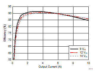
Efficiency vs Load Current
