SLVSAG3A September 2010 – December 2014 TPS61252
PRODUCTION DATA.
- 1 Features
- 2 Applications
- 3 Description
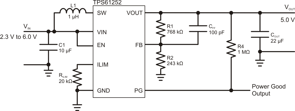
- 4 Typical Application Schematic
- 5 Revision History
- 6 Device Options
- 7 Pin Configuration and Functions
- 8 Specifications
- 9 Parameter Measurement Information
- 10Detailed Description
- 11Application and Implementation
- 12Power Supply Recommendations
- 13Layout
- 14Device and Documentation Support
- 15Mechanical, Packaging, and Orderable Information
Package Options
Mechanical Data (Package|Pins)
- DSG|8
Thermal pad, mechanical data (Package|Pins)
- DSG|8
Orderable Information
1 Features
- Resistor Programmable Input Current Limit
- ±20% Current Accuracy at 500 mA over Full Temperature Range
- Programmable from 100 mA up to 1500 mA
- Up to 92% Efficiency
- VIN Range from 2.3 V to 6.0 V
- Power Good Indicates Appropriate Output Voltage Level
- Adjustable Output Voltage up to 6.5 V
- 100% Duty-Cycle Mode When VIN > VOUT
- Load Disconnect and Reverse Current Protection
- Short Circuit Protection
- Typical Operating Frequency 3.25 MHz
- Available in a 2-mm × 2-mm WSON-8 Package
2 Applications
- USB Host Supplies from a Single Li-Ion Battery
- Current Limited Applications
- Li-Ion Applications
- Audio Applications
- RF-PA Buffer
3 Description
The TPS61252 device provides a power supply solution for products powered by either a three-cell alkaline, NiCd or NiMH battery, or an one-cell Li-Ion or Li-polymer battery. The wide input voltage range is ideal to power portable applications like mobile phones or computer peripherals. The device has a resistor programmable (RILIM) input current limit and is suitable for a wide variety of applications.
During light loads, the device automatically enters skip mode (PFM), which allows the converter to maintain the required output voltage, while only drawing 30 μA quiescent current from the battery. This allows maximum efficiency at lowest quiescent currents.
TPS61252 allows the use of small inductors and capacitors to achieve a small solution size. The possibility to reduce the current limit by a external resistor offers the potential use of physically even smaller inductors with lower rated currents to further reduce total solution sizes of the power supply. During shutdown, the load is completely disconnected from the battery. The TPS61252 is available in a 8-pin WSON package measuring 2 mm × 2 mm (DSG).
Device Information(1)
| PART NUMBER | PACKAGE | BODY SIZE (NOM) |
|---|---|---|
| TPS61252 | WSON (8) | 2.00 mm x 2.00 mm |
- For all available packages, see the orderable addendum at the end of the datasheet.
4 Typical Application Schematic