SLVS496D SEPTEMBER 2003 – August 2016 TPS65100 , TPS65101 , TPS65105
PRODUCTION DATA.
- 1 Features
- 2 Applications
- 3 Description
- 4 Revision History
- 5 Device Options
- 6 Pin Configuration and Functions
- 7 Specifications
- 8 Detailed Description
- 9 Application and Implementation
- 10Power Supply Recommendations
- 11Layout
- 12Device and Documentation Support
- 13Mechanical, Packaging, and Orderable Information
Package Options
Refer to the PDF data sheet for device specific package drawings
Mechanical Data (Package|Pins)
- RGE|24
- PWP|24
Thermal pad, mechanical data (Package|Pins)
Orderable Information
1 Features
- 2.7-V to 5.8-V Input Voltage Range
- 1.6-MHz Fixed Switching Frequency
- 3 Independent Adjustable Outputs
- Boost Converter Output Voltage VO1 of up to 15 V With < 1% Output Voltage Accuracy
- Negative Regulated Charge Pump VO2
- Positive Charge Pump VO3
- Integrated VCOM Buffer
- Virtual Synchronous Converter Technology in Boost Converter
- Auxiliary 3.3-V Linear Regulator Controller
- Internal Soft Start
- Internal Power-On Sequencing
- Fault Detection of all Outputs (TPS65100/05)
- No Fault Detection (TPS65101)
- Thermal Shutdown
- Available in TSSOP-24 and VQFN-24 PowerPAD™ Packages
2 Applications
- TFT LCD Displays for Notebooks
- TFT LCD Displays for Monitors
- Portable DVD Players
- Tablet PCs
- Car Navigation Systems
- Industrial Displays
Block Diagram

3 Description
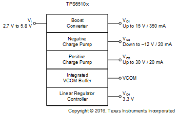
The TPS6510x series offers a compact and small power supply solution that provides all three voltages required by thin film transistor (TFT) LCD displays. The auxiliary linear regulator controller can be used to generate a 3.3-V logic power rail for systems powered by a 5-V supply rail only.
The main output VO1, is a 1.6-MHz, fixed-frequency PWM boost converter providing the source drive voltage for the LCD display. The device is available in two versions with different internal switch current limits to allow the use of a smaller external inductor when lower output power is required. The TPS65100/01 has a typical switch current limit of 2.3 A, and the TPS65105 has a typical switch current limit of 1.37 A. A fully integrated adjustable charge pump doubler/tripler provides the positive LCD gate drive voltage. An externally adjustable negative charge pump provides the negative gate drive voltage. Due to the high 1.6-MHz switching frequency of the charge pumps, inexpensive and small 220-nF capacitors can be used.
The TPS6510x series has an integrated VCOM buffer to power the LCD backplane. For LCD panels powered by 5 V only, the TPS6510x series has a linear regulator controller using an external transistor to provide a regulated 3.3-V output for the digital circuits. For maximum safety, the TPS65100/05 goes into shutdown as soon as one of the outputs is out of regulation. The device can be enabled again by toggling the input or the enable (EN) pin to GND. The TPS65101 does not enter shutdown when one of the outputs is below its power good threshold.
Device Information(1)
| PART NUMBER | PACKAGE | BODY SIZE (NOM) |
|---|---|---|
| TPS6510x | HTSSOP (24) | 7.80 mm × 4.40 mm |
| VQFN (24) | 4.00 mm × 4.00 mm |
- For all available packages, see the orderable addendum at the end of the data sheet.
4 Revision History
Changes from C Revision (April 2006) to D Revision
- Added ESD Ratings table, Thermal Information table, Feature Description section, Device Functional Modes, Application and Implementation section, Power Supply Recommendations section, Layout section, Device and Documentation Support section, and Mechanical, Packaging, and Orderable Information section Go
- Deleted Ordering Information table, see POA at the end of the datasheet. Go