SLVSAF6A June 2011 – January 2016 TPS65835
PRODUCTION DATA.
- 1 Device Overview
- 2 Revision History
- 3 Terminal Configuration and Functions
- 4 Specifications
-
5 Detailed Description
- 5.1 Overview
- 5.2 Functional Block Diagram
- 5.3 Feature Description
- 5.4 Device Functional Modes
- 5.5
MSP430 CORE
- 5.5.1
MSP430 Electrical Characteristics
- 5.5.1.1 MSP430 Recommended Operating Conditions
- 5.5.1.2 Active Mode Supply Current Into VCC Excluding External Current
- 5.5.1.3 Typical Characteristics, Active Mode Supply Current (Into VCC)
- 5.5.1.4 Low-Power Mode Supply Currents (Into VCC) Excluding External Current
- 5.5.1.5 Typical Characteristics, Low-Power Mode Supply Currents
- 5.5.1.6 Schmitt-Trigger Inputs, Ports Px
- 5.5.1.7 Leakage Current, Ports Px
- 5.5.1.8 Outputs, Ports Px
- 5.5.1.9 Output Frequency, Ports Px
- 5.5.1.10 Typical Characteristics, Outputs
- 5.5.1.11 Pin-Oscillator Frequency - Ports Px
- 5.5.1.12 Typical Characteristics, Pin-Oscillator Frequency
- 5.5.1.13 POR/Brownout Reset (BOR)
- 5.5.1.14 Typical Characteristics, POR/Brownout Reset (BOR)
- 5.5.1.15 DCO Frequency
- 5.5.1.16 Calibrated DCO Frequencies, Tolerance
- 5.5.1.17 Wake-Up From Lower-Power Modes (LPM3/4)
- 5.5.1.18 Typical Characteristics, DCO Clock Wake-Up Time From LPM3/4
- 5.5.1.19 Crystal Oscillator, XT1, Low-Frequency Mode
- 5.5.1.20 Internal Very-Low-Power Low-Frequency Oscillator (VLO)
- 5.5.1.21 Timer_A
- 5.5.1.22 USCI (UART Mode)
- 5.5.1.23 USCI (SPI Master Mode)
- 5.5.1.24 USCI (SPI Slave Mode)
- 5.5.1.25 USCI (I2C Mode)
- 5.5.1.26 Comparator_A+
- 5.5.1.27 Typical Characteristics - Comparator_A+
- 5.5.1.28 10-Bit ADC, Power Supply and Input Range Conditions
- 5.5.1.29 10-Bit ADC, Built-In Voltage Reference
- 5.5.1.30 10-Bit ADC, External Reference
- 5.5.1.31 10-Bit ADC, Timing Parameters
- 5.5.1.32 10-Bit ADC, Linearity Parameters
- 5.5.1.33 10-Bit ADC, Temperature Sensor and Built-In VMID
- 5.5.1.34 Flash Memory
- 5.5.1.35 RAM
- 5.5.1.36 JTAG and Spy-Bi-Wire Interface
- 5.5.1.37 JTAG Fuse
- 5.5.2 MSP430 Core Operation
- 5.5.1
MSP430 Electrical Characteristics
- 6 Application and Implementation
- 7 Power Supply Recommendations
- 8 Layout
- 9 Device and Documentation Support
- 10Mechanical, Packaging, and Orderable Information
Package Options
Mechanical Data (Package|Pins)
- RKP|40
Thermal pad, mechanical data (Package|Pins)
- RKP|40
Orderable Information
1 Device Overview
1.1 Features
- Power Management Core
- Linear Charger
- Three Charger Phases: Pre-Charge, Fast Charge, and Charge Termination
- LED Current Sinks for Power Good and Charger Status Indication
- Low-Dropout Regulator (LDO) Supply for External Modules & Integrated MSP430 Power
- Boost Converter
- Adjustable Output Voltage: 8 V to 16 V
- Full H-Bridge Analog Switches
- Internally Controlled by MSP430 Core for System Functions
- Linear Charger
- MSP430 Core
- Ultralow Power Consumption
- Active Mode: 280 µA at 1 MHz, 2.2 V
- Standby Mode: 0.5 µA
- Off Mode (RAM Retention): 0.1 µA
- Five Power-Saving Modes
- 16-Bit RISC Architecture
- 16-kB Flash
- Two 16-Bit Timer_A Modules with Three Capture/Compare Registers
- 10-Bit 200-ksps A/D Converter with Internal Reference, Sample-and-Hold, and Autoscan
- Universal Serial Communications Interface, Supports IrDA Encode/Decode and Synchronous SPI
- Enhanced UART Supporting Auto Baudrate Detection (LIN)
- IrDA Encoder and Decoder
- Synchronous SPI
- I2C
- Serial Onboard Programming
- No External Programming Voltage Needed
- Programmable Code Protection by Security Fuse
- For Complete Module Descriptions, See the MSP430x2xx Family User's Guide (SLAU144)
- Ultralow Power Consumption
1.2 Applications
Active Shutter 3D Glasses
1.3 Description
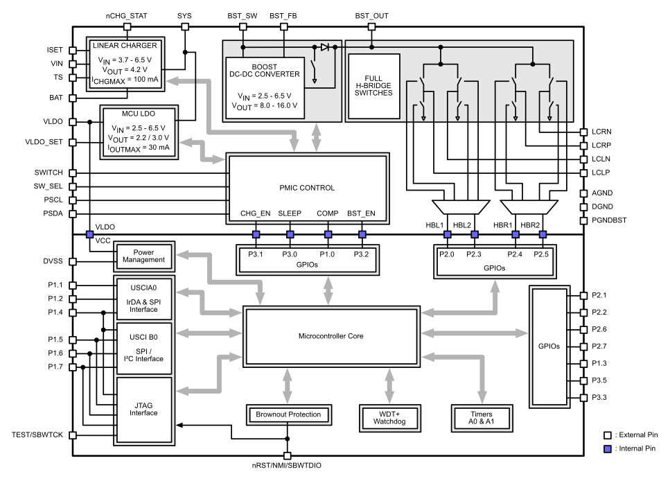
The TPS65835 is a power management unit (PMU) for active shutter 3D glasses consisting of a power management core and an MSP430 microcontroller. The power management core has an integrated power path, linear charger, LDO, boost converter, and full H-bridge analog switches for left and right shutter operation in a pair of active shutter 3D glasses. The MSP430 core supports the synchronization and communications from an IR, RF, or other communications module through the integrated universal serial communications and timer interfaces for operation of the H-bridge switches on the power management core.
Device Information(1)
| PART NUMBER | PACKAGE | BODY SIZE (NOM) |
|---|---|---|
| TPS65735 | VSON (32) | 4.00 mm x 4.00 mm |
(1) For more information, see Section 10, Mechanical Packaging and Orderable Information.
1.4 Block Diagram
 Figure 1-1 TPS65835 Simplified Functional Block Diagram