SLVSCK0A April 2014 – June 2014 TPS7A8101-Q1
PRODUCTION DATA.
- 1 Features
- 2 Applications
- 3 Description
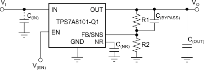
- 4 Typical Application Circuit
- 5 Revision History
- 6 Pin Configuration and Functions
- 7 Specifications
- 8 Detailed Description
- 9 Application and Implementation
- 10Power Supply Recommendations
- 11Layout
- 12Device and Documentation Support
- 13Mechanical, Packaging, and Orderable Information
Package Options
Mechanical Data (Package|Pins)
- DRB|8
Thermal pad, mechanical data (Package|Pins)
- DRB|8
Orderable Information
1 Features
- Qualified for Automotive Applications
- AEC-Q100 Qualified With the Following Results:
- Device Temperature Grade 1: –40°C to 125°C Ambient Operating Temperature Range
- Device HBM ESD Classification Level H2
- Device CDM ESD Classification Level C4B
- Low-Dropout 1-A Regulator with Enable
- Adjustable Output Voltage: 0.8 V to 6 V
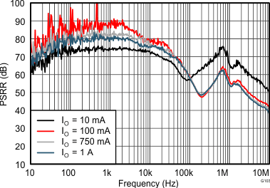
- Wide-Bandwidth High PSRR:
- 80 dB at 1 kHz
- 60 dB at 100 kHz
- 54 dB at 1 MHz
- Low Noise: 23.5 μVRMS typical (100 Hz to
100 kHz) - Stable With 4.7-μF Output Capacitance
- Excellent Load and Line Transient Response
- 3% Overall Accuracy (Over Load, Line, Temperature)
- Over-Current and Overtemperature Protection
- Very Low Dropout: 170 mV Typical at 1 A
- Package: 3-mm × 3-mm SON-8
2 Applications
- RF Power in Automotive Applications
- Automotive ADAS ECUs
- Telematic Control Units
- Audio
- High-Speed I/F (PLL and VCO)
3 Description
The TPS7A8101-Q1 low-dropout linear regulator (LDO) offers very good performance in output noise and power-supply rejection ratio (PSRR). This LDO uses an advanced BiCMOS process and a PMOSFET pass device to achieve very low noise, excellent transient response, and excellent PSRR performance.
The TPS7A8101-Q1 device is stable with a 4.7-μF ceramic output capacitor and uses a precision voltage reference and feedback loop to achieve a worst-case accuracy of 3% over all load, line, process, and temperature variations.
This device is fully specified over the temperature range of TA = –40°C to 125°C and is offered in a
3-mm × 3-mm, SON-8 package with a thermal pad.
Device Information(1)
| PART NUMBER | PACKAGE | BODY SIZE (NOM) |
|---|---|---|
| TPS7A8101-Q1 | SON (8) | 3.00 mm × 3.00 mm |
4 Typical Application Circuit
Typical Power-Supply Ripple Rejection