SLUSB36C June 2012 – January 2015 UCD8220-Q1
PRODUCTION DATA.
- 1 Features
- 2 Applications
- 3 Description
- 4 Revision History
- 5 Pin Configuration and Functions
- 6 Specifications
- 7 Detailed Description
- 8 Application and Implementation
- 9 Power Supply Recommendations
- 10Layout
- 11Device and Documentation Support
- 12Mechanical, Packaging, and Orderable Information
Package Options
Mechanical Data (Package|Pins)
- PWP|16
Thermal pad, mechanical data (Package|Pins)
- PWP|16
Orderable Information
1 Features
- AEC-Q100 Qualified With the Following Results:
- Device Temperature Grade 1: –40°C to 125°C Ambient Operating Temperature Range
- Device HBM ESD Classification Level 2
- Device CDM ESD Classification Level C4B
- For Digitally Managed Power Supplies Using μCs or the TMS320 ™ DSP Family
- Voltage or Peak Current Mode Control with Cycle-by-Cycle Current Limiting
- Clock Input from Digital Controller to Set Operating Frequency and Max Duty Cycle
- Analog PWM Comparator
- 2-MHz Switching Frequency
- 110-V Input Startup Circuit and Thermal Shutdown (UCD8620)
- Internal Programmable Slope Compensation
- 3.3-V, 10-mA Linear Regulator
- DSP/μC Compatible Inputs
- Dual ±4-A TrueDrive™ Integrated Circuit High Current Drivers
- 10-ns Typical Rise and Fall Times with 2.2-nF
- 25-ns Input-to-Output Propagation Delay
- 25-ns Current Sense-to-Output Propagation Delay
- Programmable Current-Limit Threshold
- Digital Output Current-Limit Flag
- 4.5-V to 15.5-V Supply Voltage Range
2 Applications
- Automotive HEV/EV and Powertrain
- Digitally Managed Switch Mode Power Supplies
- Push-Pull, Half-Bridge, or Full-Bridge Converters
- Battery Chargers
3 Description
The UCD8220-Q1 analog pulse-width modulator (PWM) device is used in digitally managed power supplies using a microcontroller or the TMS320 DSP family.
The UCD8220-Q1 device is a double-ended PWM controller configured with push-pull drive logic.
Systems using the UCD8220-Q1 device close the PWM feedback loop with traditional analog methods, but the UCD8220-Q1 controller includes circuitry to interpret a time-domain digital pulse train. The pulse train contains the operating frequency and maximum duty cycle limit which are used to control the power supply operation. The device circuitry eases implementation of a converter with high level control features without the added complexity or possible PWM resolution limitations of closing the control loop in the discrete time domain.
The UCD8220-Q1 device can be configured for either peak current mode or voltage mode control. The device provides a programmable current-limit function and a digital output current-limit flag which can be monitored by the host controller to set the current limit operation. For fast switching speeds, the output stage uses the TrueDrive output circuit architecture, which delivers rated current of ±4-A into the gate of a MOSFET. Finally the device also includes a 3.3-V, 10-mA linear regulator to provide power to the digital controller or act as a reference in the system.
The UCD8220-Q1 controller is compatible with the standard 3.3-V I/O ports of UCD9K digital power controllers, DSPs, microcontrollers, or ASICs and is offered in the PowerPAD™ integrated circuit package HTSSOP.
Device Information(1)
| PART NUMBER | PACKAGE | BODY SIZE (NOM) |
|---|---|---|
| UCD8220-Q1 | HTSSOP (16) | 5.00 mm × 4.40 mm |
- For all available packages, see the orderable addendum at the end of the datasheet.
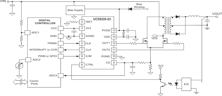
UCD8220-Q1 Typical Simplified Push-Pull Converter Application Schematic
4 Revision History
Changes from B Revision (July 2014) to C Revision
- Added the following sections to the data sheet: Device Functional Modes, Application Information, Design Requirements, Application Curves, Power Supply Recommendations, and Layout ExampleGo
- Changed the Handling Ratings table to ESD ratings and moved the storage temperature into the Absolute Maximum Ratings table Go
Changes from A Revision (June 2012) to B Revision
- Updated the data sheet format to meet the new TI data sheet standards Go
- Deleted VIN (input to internal start-up circuitry) from the Pin Functions table Go
- Added the Clearing the Current-Limit Flag (CLF) sectionGo
Changes from * Revision (June 2012) to A Revision
- Device went from preview to productionGo