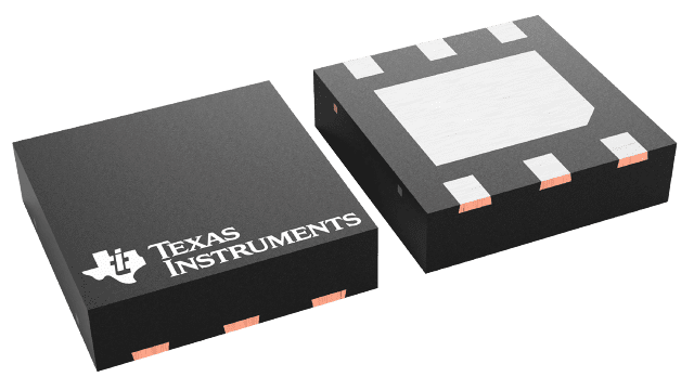
Información de empaque
| Encapsulado | Pines WSON (NGG) | 6 |
| Rango de temperatura de funcionamiento (℃) -40 to 125 |
| Cant. de paquetes | Empresa de transporte 4,500 | LARGE T&R |
Características para LM5114
- Independent Source and Sink Outputs for
Controllable Rise and Fall Times - 4-V to 12.6-V Single Power Supply
- 7.6-A/1.3-A Peak Sink and Source Drive Current
- 0.23-Ω Open-drain Pulldown Sink Output
- 2-Ω Open-drain Pullup Source Output
- 12-ns (Typical) Propagation Delay
- Matching Delay Time Between Inverting and
Noninverting Inputs - TTL/CMOS Logic Inputs
- 0.68-V Input Hysteresis
- Up to 14-V Logic Inputs (Regardless of VDD Voltage)
- Low Input Capacitance: 2.5-pF (Typical)
- –40°C to 125°C Operating Temperature Range
- Pin-to-Pin Compatible With MAX5048
- 6-Pin SOT-23
Descripción de LM5114
The LM5114 is designed to drive low-side MOSFETs in boost-type configurations or to drive secondary synchronous MOSFETs in isolated topologies. With strong sink current capability, the LM5114 can drive multiple FETs in parallel. The LM5114 also has the features necessary to drive low-side enhancement mode Gallium Nitride (GaN) FETs. The LM5114 provides inverting and noninverting inputs to satisfy requirements for inverting and Noninverting gate drive in a single device type. The inputs of the LM5114 are TTL/CMOS Logic compatible and withstand input voltages up to 14 V regardless of the VDD voltage. The LM5114 has split gate outputs, providing flexibility to adjust the turnon and turnoff strength independently. The LM5114 has fast switching speed and minimized propagation delays, facilitating high-frequency operation. The LM5114 is available in a 6-pin SOT-23 package and a 6-pin WSON package with an exposed pad to aid thermal dissipation.
