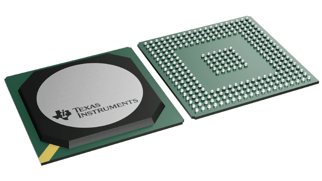
封裝資訊
| 封裝 | 引腳 BGA (NXA) | 292 |
| 作業溫度範圍 (°C) -40 to 85 |
| 包裝數量 | 運送包裝 40 | JEDEC TRAY (10+1) |
ADC12D1000RF 的特色
- Excellent Noise and Linearity up to and Above fIN =
2.7 GHz - Configurable to Either 3.2 or 2 GSPS Interleaved
or 1600 or 1000 MSPS Dual ADC - New DESCLKIQ Mode for High Bandwidth, High
Sampling Rate Apps - Pin-Compatible With ADC10D1x00, ADC12D1x00
- AutoSync Feature for Multi-Chip Synchronization
- Internally Terminated, Buffered, Differential Analog
Inputs - Interleaved Timing Automatic and Manual Skew
Adjust - Test Patterns at Output for System Debug
- Time Stamp Feature to Capture External Trigger
- Programmable Gain, Offset, and tAD Adjust
Feature - 1:1 Non-Demuxed or 1:2 Demuxed LVDS Outputs
- Key Specifications
- Resolution 12 Bits
- Interleaved 3.2- and 2-GSPS ADC
- IMD3 (Fin = 2.7 GHz at –13 dBFS) –63.7/–73
dBFS (Typical) - IMD3 (Fin = 2.7 GHz at –16 dBFS) –66.7/–85
dBFS (Typical) - Noise Floor –154.6/–154 dBm/Hz (Typical)
- Power 3.94/3.42 W (Typical)
- IMD3 (Fin = 2.7 GHz at –13 dBFS) –63.7/–73
- Dual 1600/1000 MSPS ADC, Fin = 498 MHz
- ENOB 9.2/9.4 Bits (Typical)
- SNR 58.2/58.8 dB (Typical)
- SFDR 66.7/71.9 dBc (Typical)
- Power per Channel 1.97/1.71 W (Typical)
ADC12D1000RF 的說明
The 12-bit 3.2- and 2-GSPS ADC12D1x00RF is an RF-sampling GSPS ADC that can directly sample input frequencies up to and above 2.7 GHz. The ADC12D1x00RF augments the very large Nyquist zone of TI’s GSPS ADCs with excellent noise and linearity performance at RF frequencies, extending its usable range beyond the 3rd Nyquist zone
The ADC12D1x00RF provides a flexible LVDS interface which has multiple SPI programmable options to facilitate board design and FPGA/ASIC data capture. The LVDS outputs are compatible with IEEE 1596.3-1996 and supports programmable common-mode voltage. The product is packaged in a lead-free 292-ball thermally enhanced BGA package over the rated industrial temperature range of –40°C to 85°C.
