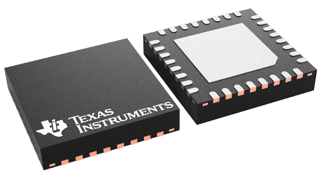
封裝資訊
| 封裝 | 引腳 VQFN (RHB) | 32 |
| 作業溫度範圍 (°C) -40 to 85 |
| 包裝數量 | 運送包裝 3,000 | LARGE T&R |
CDCLVC1310 的特色
- High-Performance Crystal Buffer With Ultralow Noise
Floor of –169 dBc/Hz - Additive Phase Noise/Jitter Performance Is
25 fsRMS (Typ.) - Level Translation With 3.3-V or 2.5-V Core and
3.3-V, 2.5-V, 1.8-V, or 1.5-V Output Supply - Device inputs consist of primary, secondary,
and crystal inputs, and manually selectable
(through pins) using the input MUX. The primary
and secondary inputs can accept LVPECL, LVDS,
HCSL, SSTL or LVCMOS signals and crystal input.- Crystal Frequencies Supported Are From
8 MHz to 50 MHz - Differential and Single-Ended Input Frequencies
Supported Are up to 200 MHz
- Crystal Frequencies Supported Are From
- 10 Single-Ended LVCMOS Outputs. The outputs can
operate at 1.5-V, 1.8-V, 2.5-V or 3.3-V
Power-Supply Voltage.- LVCMOS Outputs Operate up to 200 MHz
- Output Skew Is 30 ps (Typical)
- Total Propagation Delay Is 2 ns (Typical)
- Synchronous and Glitch-Free Output Enable Is
Available
- Offered in QFN-32 5-mm × 5-mm Package With
Industrial Temperature Range of –40°C to 85°C - Can Overdrive Crystal Input With LVCMOS Signal up to 50 MHz
CDCLVC1310 的說明
The CDCLVC1310 is a highly versatile, low-jitter, low-power clock fanout buffer which can distribute to ten low-jitter LVCMOS clock outputs from one of three inputs, whose primary and secondary inputs can feature differential or single-ended signals and crystal input. Such a buffer is good for use in a variety of mobile and wired infrastructure, data communication, computing, low-power medical imaging, and portable test and measurement applications. When the input is an illegal level, the output is at a defined state. One can set the core to 2.5 V or 3.3 V, and output to 1.5 V, 1.8 V, 2.5 V or 3.3 V. Pin programming easily configures the CDCLVC1310. The overall additive jitter performance is 25 fsRMS (typical). The CDCLVC1310 comes in a small 32-pin 5-mm × 5-mm QFN package.
