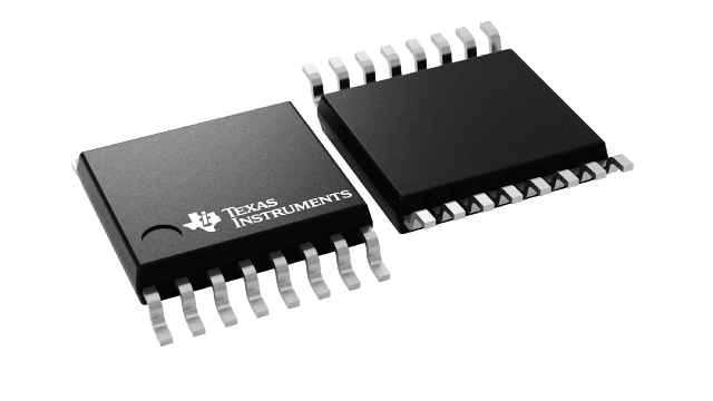
封裝資訊
| 封裝 | 引腳 TSSOP (PW) | 16 |
| 作業溫度範圍 (°C) -40 to 125 |
| 包裝數量 | 運送包裝 2,000 | LARGE T&R |
SN3257-Q1 的特色
- Functional safety-capable
- AEC-Q100 qualified for automotive application
- Temperature grade 1: -40°C to +125°C, TA
- Wide supply range: 1.5 V to 5.5 V
- Low propagation delay: 78 ps
- Low on-resistance: 5 Ω
- High bandwidth: 2 GHz
- Bidirectional signal path
- Supports input voltage beyond supply
- 1.8 V logic compatible
- Integrated pull down resistor on logic pins
- Fail-safe logic
- Powered-off protection up to 3.6 V signals
SN3257-Q1 的說明
The SN3257-Q1 is an automotive grade complementary metal-oxide semiconductor (CMOS) switch that supports high speed signals with low propagation delay. The SN3257-Q1 offers a 2:1 (SPDT) switch configuration with 4-channels making it ideal for multi-lane protocols such as SPI and I2S. The device supports bidirectional analog and digital signals on the source (SxA, SxB) and drain (Dx) pins and can pass signals above supply up to VDD x 2, with a maximum input and output voltage of 5.5 V.
The SN3257-Q1 has an active low EN pin that is used to enable and disable all channels simultaneously. When the EN pin is LOW, one of the two switch paths is selected based on the state of SEL pin.
Powered-off protection up to 3.6 V on the signal path of the SN3257-Q1 provides isolation when the supply voltage is removed (VDD = 0 V). Without this protection feature, switches can back-power the supply rail through an internal ESD diode and cause potential damage to the system.
Fail-safe logic circuitry allows voltages on the logic control pins to be applied before the supply pin, protecting the device from potential damage. Both logic control inputs have 1.8 V logic compatible thresholds, ensuring both TTL and CMOS logic compatibility. Integrated pull down resistor on the logic pins removes external components to reduce system size and cost.
