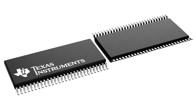
封裝資訊
| 封裝 | 引腳 TSSOP (DGG) | 56 |
| 作業溫度範圍 (°C) -40 to 85 |
| 包裝數量 | 運送包裝 2,000 | LARGE T&R |
SN74ALVCF162835 的特色
- Member of the Texas Instruments Widebus™ Family
- Ideal for Use in PC133 Register DIMM
- Typical Output Skew . . . <250 ps
- VCC = 3.3 V ± 0.3 V . . . Normal Range
- VCC = 2.7 V to 3.6 V . . . Extended Range
- VCC = 2.5 V ± 0.2 V
- Rail-to-Rail Output Swing for Increased Noise Margin
- Balanced Output Drivers . . . ±18 mA
- Low Switching Noise
- Latch-Up Performance Exceeds 100 mA Per JESD 78, Class II
- ESD Protection Exceeds JESD 22
- 2000-V Human-Body Model (A114-A)
- 200-V Machine Model (A115-A)
- 1000-V Charged-Device Model (C101)
Widebus is a trademark of Texas Instruments.
SN74ALVCF162835 的說明
This 18-bit universal bus driver is designed for 2.3-V to 3.6-V VCC operation.
Data flow from A to Y is controlled by the output-enable (OE)\ input. The device operates in the transparent mode when the latch-enable (LE) input is high. When LE is low, the A data is latched if the clock (CLK) input is held at a high or low logic level. If LE is low, the A data is stored in the latch/flip-flop on the low-to-high transition of CLK. When OE\ is high, the outputs are in the high-impedance state.
The SN74ALVCF162835 has series damping resistors in the device output structure that reduce switching noise in 128-MB and 256-MB SDRAM modules. Designed with a drive capability of ±18 mA, this device is a midway drive between the SN74ALVC162835 (±12 mA) and SN74ALVC16835 (±24 mA).
The SN74ALVCF162835 is a faster version of the SN74ALVC162835. It is suitable for PC133 applications and, particularly, SDRAM modules clocked at 133 MHz.
To ensure the high-impedance state during power up or power down, OE\ should be tied to VCC through a pullup resistor; the minimum value of the resistor is determined by the current-sinking capability of the driver.
