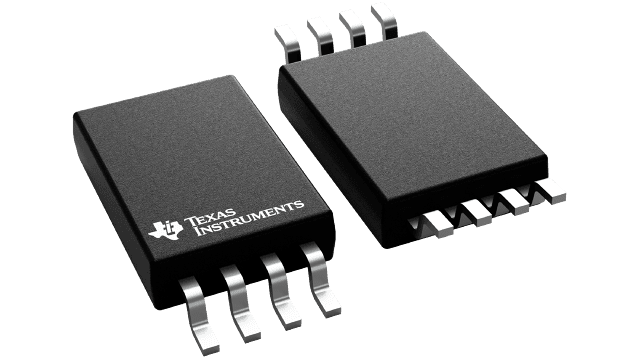
封裝資訊
| 封裝 | 引腳 TSSOP (PW) | 8 |
| 作業溫度範圍 (°C) -40 to 85 |
| 包裝數量 | 運送包裝 2,000 | LARGE T&R |
SN74CB3Q3305 的特色
- High-bandwidth data path (up to 500 MHz)(1)
- 5-V tolerant I/Os with device powered up or powered down
- Low and flat ON-state resistance (ron) characteristics over operating range (ron = 3 Ω typical)
- Supports input voltage beyond supply on data I/O ports
- 0 to 5 V switching with 3.3 V VCC
- 0 to 3.3 V switching with 2.5 V VCC
- Bidirectional data flow with near-zero propagation delay
- Low input or output capacitance minimizes loading and signal distortion (Cio(OFF) = 3.5 pF typical)
- Fast switching frequency (fOE = 20 MHz maximum)
- Data and control inputs provide undershoot clamp diodes
- Low power consumption (ICC = 0.25 mA typical)
- VCC operating range from 2.3 V to 3.6 V
- Data I/Os support 0 to 5 V signaling levels (0.8 V, 1.2 V, 1.5 V, 1.8 V, 2.5 V, 3.3 V, and 5 V)
- Control inputs can be driven by TTL or 5 V/3.3 V CMOS outputs
- Ioff supports partial-power-down mode operation
- Latch-up performance exceeds 100 mA per JESD 78, Class II
(1)For additional information regarding the performance characteristics of the CB3Q family, refer to the TI application report, CBT-C, CB3T, and CB3Q Signal-Switch Families, SCDA008.
SN74CB3Q3305 的說明
The SN74CB3Q3305 device is a high-bandwidth FET bus switch using a charge pump to elevate the gate voltage of the pass transistor, providing a low and flat ON-state resistance (ron). The low and flat ON-state resistance allows for minimal propagation delay and supports switching input voltage beyond the supply on the data input/output (I/O) ports. The device also features low data I/O capacitance to minimize capacitive loading and signal distortion on the data bus. Specifically designed to support high-bandwidth applications, the SN74CB3Q3305 device provides an optimized interface solution ideally suited for broadband communications, networking, and data-intensive computing systems.
This device is fully specified for partial-power-down applications using Ioff. The Ioff circuitry prevents damaging current backflow through the device when it is powered down. The device has isolation during power off.
To ensure the high-impedance state during power up or power down, OE should be tied to GND through a pulldown resistor; the minimum value of the resistor is determined by the current-sourcing capability of the driver.
