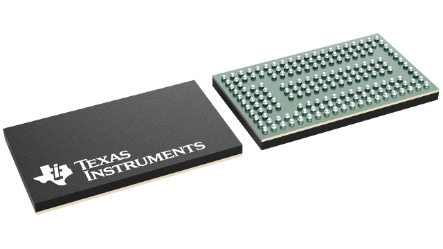
封裝資訊
| 封裝 | 引腳 NFBGA (ZAL) | 176 |
| 作業溫度範圍 (°C) 0 to 85 |
| 包裝數量 | 運送包裝 2,000 | LARGE T&R |
SN74SSQEC32882 的特色
- JEDEC SSTE32882
- 1-to-2 Register Outputs and 1-to-4 Clock Pair Outputs Support
Stacked DDR3 RDIMMs - CKE Powerdown Mode for Optimized System Power Consumption
- 1.5V/1.35V/1.25V Phase Lock Loop Clock Driver for Buffering
One Differential Clock Pair (CK and CK)
and Distributing to Four Differential Outputs - 1.5V/1.35V/1.25V CMOS Inputs
- Checks Parity on Command and Address (CS-Gated) Data Inputs
- Configurable Driver Strength
- Uses Internal Feedback Loop
- Optimized Power Consumption
SN74SSQEC32882 的說明
This 1:2 or 26-bit 1:2 and 4-bit 1:1 registering clock driver with parity is designed for operation on DDR3 registered DIMMs with VDD of 1.5 V, on DDR3L registered DIMMs with VDD of 1.35 V and on DDR3U registered DIMMs with VDD of 1.25 V.
All inputs are 1.5 V, 1.35V and 1.25 V CMOS compatible. All outputs are CMOS drivers optimized to drive DRAM signals on terminated traces in DDR3 RDIMM applications. The clock outputs Yn and Yn and control net outputs DxCKEn, DxCSn and DxODTn can be driven with a different strength and skew to optimize signal integrity, compensate for different loading and equalize signal travel speed.
The SN74SSQEC32882 has two basic modes of operation associated with the Quad Chip Select Enable (QCSEN) input. When the QCSEN input pin is open (or pulled high), the component has two chip select inputs, DCS0 and DCS1, and two copies of each chip select output, QACS0, QACS1, QBCS0 and QBCS1. This is the "QuadCS disabled" mode. When the QCSEN input pin is pulled low, the component has four chip select inputs DCS[3:0], and four chip select outputs, QCS[3:0]. This is the "QuadCS enabled" mode. Through the remainder of this specification, DCS[n:0] will indicate all of the chip select inputs, where n=1 for QuadCS disabled, and n=3 for QuadCS enabled. QxCS[n:0] will indicate all of the chip select outputs.
The device also supports a mode where a single device can be mounted on the back side of a DIMM. If MIRROR=HIGH, Input Bus Termination (IBT) has to stay enabled for all input signals in this case.
The SN74SSQEC32882 operates from a differential clock (CK and CK). Data are registered at the crossing of CK going HIGH, and CK going LOW. This data could be either re-driven to the outputs or it could be used to access device internal control registers.
The input bus data integrity is protected by a parity function. All address and command input signals are added up and the last bit of the sum is compared to the parity signal delivered by the system at the input PAR_IN one clock cycle later. If they do not match the device pulls the open drain output ERROUT LOW. The control signals (DCKE0, DCKE1, DODT0, DODT1, DCS[n:0]) are not part of this computation.
The SN74SSQEC32882 implements different power saving mechanisms to reduce thermal power dissipation and to support system power down states. By disabling unused outputs the power consumption is further reduced.
The package is optimized to support high density DIMMs. By aligning input and output positions towards DIMM finger signal ordering and SDRAM ballout the device de-scrambles the DIMM traces allowing low cross talk design with low interconnect latency.
Edge controlled outputs reduce ringing and improve signal eye opening at the SDRAM inputs.
