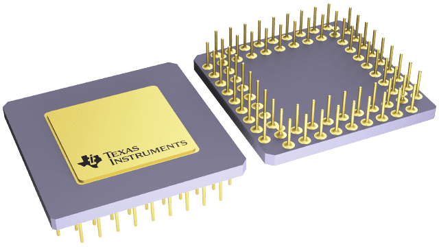
封裝資訊
| 封裝 | 引腳 CPGA (GB) | 68 |
| 作業溫度範圍 (°C) -40 to 85 |
| 包裝數量 | 運送包裝 21 | JEDEC TRAY (10+1) |
TMS320C25 的特色
- 80-ns Instruction Cycle Time
- 544 Words of On-Chip Data RAM
- 4K Words of On-Chip Secure Program EPROM (TMS320E25)
- 4K Words of On-Chip Program ROM (TMS320C25)
- 128K Words of Data/Program Space
- 32-Bit ALU/Accumulator
- 16 × 16-Bit Multiplier With a 32-Bit Product
- Block Moves for Data/Program Management
- Repeat Instructions for Efficient Use of Program Space
- Serial Port for Direct Codec Interface
- Synchronization Input for Synchronous Multiprocessor Configurations
- Wait States for Communication to Slow Off-Chip Memories/Peripherals
- On-Chip Timer for Control Operations
- Single 5-V Supply
- Packaging: 68-Pin PGA, PLCC, and CER-QUAD
- 68-to-28 Pin Conversion Adapter Socket for EPROM Programming
- Commercial and Military Versions Available
- NMOS Technology:
TMS32020 . . . 200-ns cycle time - CMOS Technology:
TMS320C25 . . . 100-ns cycle time
TMS320E25 . . . 100-ns cycle time
TMS320C25-50 . . . 80-ns cycle time
TMS320C25 的說明
This data sheet provides complete design documentation for the second-generation devices of the TMS320 family. This facilitates the selection of the devices best suited for user applications by providing all specifications and special features for each TMS320 member. This data sheet is divided into four major sections: architecture, electrical specifications (NMOS and CMOS), timing diagrams, and mechanical data. In each of these sections, generic information is presented first, followed by specific device information. An index is provided for quick reference to specific information about a device.
The TMS320 family of 16/32-bit single-chip digital signal processors combines the flexibility of a high-speed controller with the numerical capability of an array processor, thereby offering an inexpensive alternative to multichip bit-slice processors. The highly paralleled architecture and efficient instruction set provide speed and flexibility to produce a MOS microprocessor family that is capable of executing more than 12.5 MIPS (million instructions per section). The TMS320 family optimizes speed by implementing functions in hardware that other processors implement through microcode or software. This hardware-intensive approach provides the design engineer with processing power previously unavailable on a single chip.
The TMS320 family consists of three generations of digital signal processors. The first generation contains the TMS32010 and its spinoffs. The second generation includes the TMS32020, TMS320C25, and TMS320E25, which are described in this data sheet. The TMS320C30 is a floating-point DSP device designed for even higher performance. Many features are common among the TMS320 processors. Specific features are added in each processor to provide different cost/performance tradeoffs. Software compatibility is maintained throughout the family to protect the user's investment in architecture. Each processor has software and hardware tools to facilitate rapid design.