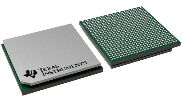
封裝資訊
| 封裝 | 引腳 FCBGA (GZH) | 625 |
| 作業溫度範圍 (°C) -40 to 100 |
| 包裝數量 | 運送包裝 60 | JEDEC TRAY (5+1) |
TMS320C6655 的特色
- One (C6655) or Two (C6657) TMS320C66x™ DSP Core Subsystems
(CorePacs), Each With
- 850 MHz (C6657 only), 1.0 GHz, or 1.25 GHz C66x Fixed- and Floating-Point CPU
Core
- 40 GMAC per Core for Fixed Point @ 1.25 GHz
- 20 GFLOP per Core for Floating Point @ 1.25 GHz
- 850 MHz (C6657 only), 1.0 GHz, or 1.25 GHz C66x Fixed- and Floating-Point CPU
Core
- Multicore Shared Memory
Controller (MSMC)
- 1024KB MSM SRAM Memory
(Shared by Two DSP C66x CorePacs for C6657) - Memory Protection Unit for Both MSM SRAM and DDR3_EMIF
- 1024KB MSM SRAM Memory
- Multicore Navigator
- 8192 Multipurpose Hardware Queues with Queue Manager
- Packet-Based DMA for Zero-Overhead Transfers
- Hardware Accelerators
- Two Viterbi Coprocessors
- One Turbo Coprocessor Decoder
- Peripherals
- Four Lanes of SRIO 2.1
- 1.24, 2.5, 3.125, and 5 GBaud Operation Supported Per Lane
- Supports Direct I/O, Message Passing
- Supports Four 1×, Two 2×, One 4×, and Two 1× + One 2× Link Configurations
- PCIe Gen2
- Single Port Supporting 1 or 2 Lanes
- Supports up to 5 GBaud Per Lane
- HyperLink
- Supports Connections to Other KeyStone Architecture Devices Providing Resource Scalability
- Supports up to 40 Gbaud
- Gigabit Ethernet (GbE) Subsystem
- One SGMII Port
- Supports 10-, 100-, and 1000-Mbps Operation
- 32-Bit DDR3 Interface
- DDR3-1333
- 4GB of Addressable Memory Space
- 16-Bit EMIF
- Universal Parallel Port
- Two Channels of 8 Bits or 16 Bits Each
- Supports SDR and DDR Transfers
- Two UART Interfaces
- Two Multichannel Buffered Serial Ports (McBSPs)
- I2C Interface
- 32 GPIO Pins
- SPI Interface
- Semaphore Module
- Up to Eight 64-Bit Timers
- Two On-Chip PLLs
- Four Lanes of SRIO 2.1
- Commercial Temperature:
- 0°C to 85°C
- Extended Temperature:
- –40°C to 100°C
TMS320C6655 的說明
The C665x are high performance fixed- and floating-point DSPs that are based on TI’s KeyStone multicore architecture. Incorporating the new and innovative C66x DSP core, this device can run at a core speed of up to 1.25 GHz. For developers of a broad range of applications, both C665x DSPs enable a platform that is power-efficient and easy to use. In addition, the C665x DSPs are fully backward compatible with all existing C6000™ family of fixed- and floating-point DSPs.
TI’s KeyStone architecture provides a programmable platform integrating various subsystems (C66x cores, memory subsystem, peripherals, and accelerators) and uses several innovative components and techniques to maximize intradevice and interdevice communication that lets the various DSP resources operate efficiently and seamlessly. Central to this architecture are key components such as Multicore Navigator that allows for efficient data management between the various device components. The TeraNet is a nonblocking switch fabric enabling fast and contention-free internal data movement. The multicore shared memory controller allows access to shared and external memory directly without drawing from switch fabric capacity.
For fixed-point use, the C66x core has 4× the multiply accumulate (MAC) capability of C64x+ cores. In addition, the C66x core integrates floating-point capability and the per-core raw computational performance is an industry-leading 40 GMACS per core and 20 GFLOPS per core (@1.25 GHz operating frequency). The C66x core can execute 8 single precision floating-point MAC operations per cycle and can perform double- and mixed-precision operations and is IEEE 754 compliant. The C66x core incorporates 90 new instructions (compared to the C64x+ core) targeted for floating-point and vector math oriented processing. These enhancements yield sizeable performance improvements in popular DSP kernels used in signal processing, mathematical, and image acquisition functions. The C66x core is backward code-compatible with TI’s previous generation C6000 fixed- and floating-point DSP cores, ensuring software portability and shortened software development cycles for applications migrating to faster hardware.
The C665x DSP integrates a large amount of on-chip memory. In addition to 32KB of L1 program and data cache, 1024KB of dedicated memory can be configured as mapped RAM or cache. The device also integrates 1024KB of Multicore Shared Memory that can be used as a shared L2 SRAM and/or shared L3 SRAM. All L2 memories incorporate error detection and error correction. For fast access to external memory, this device includes a 32-bit DDR-3 external memory interface (EMIF) running at a rate of 1333 MHz and has ECC DRAM support.
This family supports a number of high-speed standard interfaces including RapidIO ver 2, PCI Express Gen2, and Gigabit Ethernet. This family of DSPs also includes I2C, UART, Multichannel Buffered Serial Port (McBSP), Universal Parallel Port (uPP), and a 16-bit asynchronous EMIF, along with general-purpose CMOS IO. For high throughput, low latency communication between devices or with an FPGA, a 40-Gbaud full-duplex interface called HyperLink is included.
The C665x devices have a complete set of development tools, which includes: an enhanced C compiler, an assembly optimizer to simplify programming and scheduling, and a Windows® debugger interface for visibility into source code execution.
TI’s KeyStone Multicore Architecture provides a high performance structure for integrating RISC and DSP cores with application-specific coprocessors and I/O. The KeyStone architecture is the first of its kind that provides adequate internal bandwidth for nonblocking access to all processing cores, peripherals, coprocessors, and I/O. This internal bandwidth is achieved with four main hardware elements: Multicore Navigator, TeraNet, Multicore Shared Memory Controller, and HyperLink.
Multicore Navigator is an innovative packet-based manager that controls 8192 queues. When tasks are allocated to the queues, Multicore Navigator provides hardware-accelerated dispatch that directs tasks to the appropriate available hardware. The packet-based system on a chip (SoC) uses the two Tbps capacity of the TeraNet switched central resource to move packets. The Multicore Shared Memory Controller lets processing cores access shared memory directly without drawing from the capacity of TeraNet, so packet movement cannot be blocked by memory access.
HyperLink provides a 40-Gbaud chip-level interconnect that lets SoCs work in tandem. The low-protocol overhead and high throughput of HyperLink make an ideal interface for chip-to-chip interconnections. Working with Multicore Navigator, HyperLink dispatches tasks to tandem devices transparently and executes tasks as if they are running on local resources.