封裝資訊
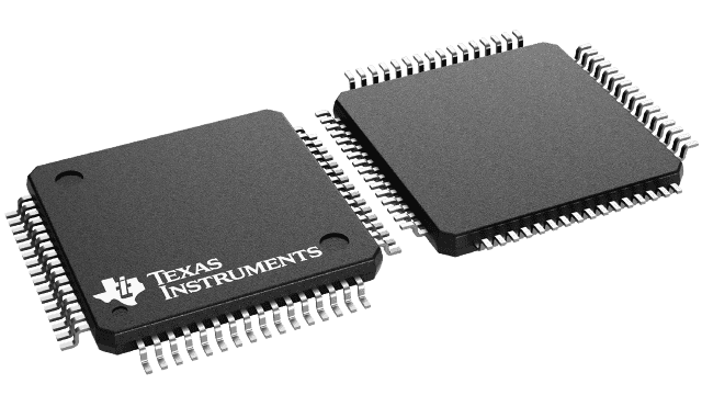
| 封裝 | 引腳 TQFP (PAG) | 64 |
| 作業溫度範圍 (°C) -40 to 85 |
| 包裝數量 | 運送包裝 160 | JEDEC TRAY (5+1) |
TMS320LF2403A 的特色
- High-Performance Static CMOS Technology
- 25-ns Instruction Cycle Time (40 MHz)
- 40-MIPS Performance
- Low-Power 3.3-V Design
- Based on TMS320C2xx DSP CPU Core
- Code-Compatible With F243/F241/C242
- Instruction Set and Module Compatible With F240
- Flash (LF) and ROM (LC) Device Options
- LF240xA: LF2407A, LF2406A, LF2403A, LF2402A
- LC240xA: LC2406A, LC2404A, LC2403A, LC2402A
- On-Chip Memory
- Up to 32K Words x 16 Bits of Flash EEPROM (4 Sectors) or ROM
- Programmable "Code-Security" Feature for the On-Chip Flash/ROM
- Up to 2.5K Words x 16 Bits of Data/Program RAM
- 544 Words of Dual-Access RAM
- Up to 2K Words of Single-Access RAM
- Boot ROM (LF240xA Devices)
- SCI/SPI Bootloader
- Up to Two Event-Manager (EV) Modules (EVA and EVB), Each Includes:
- Two 16-Bit General-Purpose Timers
- Eight 16-Bit Pulse-Width Modulation (PWM) Channels Which Enable:
- Three-Phase Inverter Control
- Center- or Edge-Alignment of PWM Channels
- Emergency PWM Channel Shutdown With External PDPINTx Pin
- Programmable Deadband (Deadtime) Prevents Shoot-Through Faults
- Three Capture Units for Time-Stamping of External Events
- Input Qualifier for Select Pins
- On-Chip Position Encoder Interface Circuitry
- Synchronized A-to-D Conversion
- Designed for AC Induction, BLDC, Switched Reluctance, and Stepper Motor Control
- Applicable for Multiple Motor and/or Converter Control
- External Memory Interface (LF2407A)
- 192K Words x 16 Bits of Total Memory: 64K Program, 64K Data, 64K I/O
- Watchdog (WD) Timer Module
- 10-Bit Analog-to-Digital Converter (ADC)
- 8 or 16 Multiplexed Input Channels
- 500 ns MIN Conversion Time
- Selectable Twin 8-State Sequencers Triggered by Two Event Managers
- Controller Area Network (CAN) 2.0B Module (LF2407A, 2406A, 2403A)
- Serial Communications Interface (SCI)
- 16-Bit Serial Peripheral Interface (SPI) (LF2407A, 2406A, LC2404A, 2403A)
- Phase-Locked-Loop (PLL)-Based Clock Generation
- Up to 40 Individually Programmable, Multiplexed General-Purpose Input/Output (GPIO) Pins
- Up to Five External Interrupts (Power Drive Protection, Reset, Two Maskable Interrupts)
- Power Management:
- Three Power-Down Modes
- Ability to Power Down Each Peripheral Independently
- Real-Time JTAG-Compliant Scan-Based Emulation, IEEE Standard 1149.1
 (JTAG)
 - Development Tools Include:
- Texas Instruments (TI) ANSI C Compiler, Assembler/Linker, and Code Composer Studio™; Debugger
- Evaluation Modules
- Scan-Based Self-Emulation (XDS510™;)
- Broad Third-Party Digital Motor Control Support
- Package Options
- 144-Pin LQFP PGE (LF2407A)
- 100-Pin LQFP PZ (2406A, LC2404A)
- 64-Pin TQFP PAG (LF2403A, LC2403A, LC2402A)
- 64-Pin QFP PG (2402A)
- Extended Temperature Options (A and S)
- A: –40°C to 85°C
- S: –40°C to 125°C
Code Composer Studio and XDS510 are trademarks of Texas Instruments.
Other trademarks are the property of their respective owners.
IEEE Standard 1149.1-1990, IEEE Standard Test-Access Port
TMS320C24x, TMS320C2000, TMS320, and C24x are trademarks of Texas Instruments.
TMS320LF2403A 的說明
The TMS320LF240xA and TMS320LC240xA devices, new members of the TMS320C24x™; generation of digital signal processor (DSP) controllers, are part of the TMS320C2000™; platform of fixed-point DSPs. The 240xA devices offer the enhanced TMS320™; DSP architectural design of the C2xx core CPU for low-cost, low-power, and high-performance processing capabilities. Several advanced peripherals, optimized for digital motor and motion control applications, have been integrated to provide a true single-chip DSP controller. While code-compatible with the existing C24x™; DSP controller devices, the 240xA offers increased processing performance (40 MIPS) and a higher level of peripheral integration. See the TMS320x240xA Device Summary section for device-specific features.
The 240xA generation offers an array of memory sizes and different peripherals tailored to meet the specific price/performance points required by various applications. Flash devices of up to 32K words offer a cost-effective reprogrammable solution for volume production. The 240xA devices offer a password-based "code security" feature which is useful in preventing unauthorized duplication of proprietary code stored in on-chip Flash/ROM. Note that Flash-based devices contain a 256-word boot ROM to facilitate in-circuit programming. The 240xA family also includes ROM devices that are fully pin-to-pin compatible with their Flash counterparts.
All 240xA devices offer at least one event manager module which has been optimized for digital motor control and power conversion applications. Capabilities of this module include center- and/or edge-aligned PWM generation, programmable deadband to prevent shoot-through faults, and synchronized analog-to-digital conversion. Devices with dual event managers enable multiple motor and/or converter control with a single 240xA DSP controller. Select EV pins have been provided with an "input-qualifier" circuitry, which minimizes inadvertent pin-triggering by glitches.
The high-performance, 10-bit analog-to-digital converter (ADC) has a minimum conversion time of 375 ns and offers up to 16 channels of analog input. The autosequencing capability of the ADC allows a maximum of 16 conversions to take place in a single conversion session without any CPU overhead.
A serial communications interface (SCI) is integrated on all devices to provide asynchronous communication to other devices in the system. For systems requiring additional communication interfaces, the 2407A, 2406A, 2404A, and 2403A offer a 16-bit synchronous serial peripheral interface (SPI). The 2407A, 2406A, and 2403A offer a controller area network (CAN) communications module that meets 2.0B specifications. To maximize device flexibility, functional pins are also configurable as general-purpose inputs/outputs (GPIOs).
To streamline development time, JTAG-compliant scan-based emulation has been integrated into all devices. This provides non-intrusive real-time capabilities required to debug digital control systems. A complete suite of code-generation tools from C compilers to the industry-standard Code Composer Studio™; debugger supports this family. Numerous third-party developers not only offer device-level development tools, but also system-level design and development support.