封裝資訊
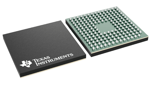
| 封裝 | 引腳 NFBGA (GBB) | 179 |
| 作業溫度範圍 (°C) -40 to 85 |
| 包裝數量 | 運送包裝 160 | JEDEC TRAY (5+1) |
TMS320VC5509A 的特色
- High-Performance, Low-Power, Fixed-Point TMS320C55™ Digital Signal Processor
- 9.26-, 6.95-, 5-ns Instruction Cycle Time
- 108-, 144-, 200-MHz Clock Rate
- One/Two Instruction(s) Executed per Cycle
- Dual Multipliers [Up to 400 Million Multiply-Accumulates per Second (MMACS)]
- Two Arithmetic/Logic Units (ALUs)
- Three Internal Data/Operand Read Buses and Two Internal Data/Operand Write Buses
- 128K × 16-Bit On-Chip RAM, Composed of:
- 64K Bytes of Dual-Access RAM (DARAM) 8 Blocks of 4K × 16-Bit
- 192K Bytes of Single-Access RAM (SARAM) 24 Blocks of 4K × 16-Bit
- 64K Bytes of One-Wait-State On-Chip ROM (32K × 16-Bit)
- 8M × 16-Bit Maximum Addressable External Memory Space (Synchronous DRAM)
- 16-Bit External Parallel Bus Memory Supporting Either:
- External Memory Interface (EMIF) With GPIO Capabilities and Glueless Interface to:
- Asynchronous Static RAM (SRAM)
- Asynchronous EPROM
- Synchronous DRAM (SDRAM)
- External Memory Interface (EMIF) With GPIO Capabilities and Glueless Interface to:
- 16-Bit Parallel Enhanced Host-Port Interface (EHPI) With GPIO Capabilities
- Two 20-Bit Timers
- Watchdog Timer
- Six-Channel Direct Memory Access (DMA) Controller
- Three Serial Ports Supporting a Combination of:
- Up to 3 Multichannel Buffered Serial Ports (McBSPs)
- Up to 2 MultiMedia/Secure Digital CardInterfaces
- Programmable Phase-Locked Loop Clock Generator
- Seven (LQFP) or Eight (BGA) General-Purpose I/O (GPIO) Pins and a General- Purpose Output Pin (XF)
- USB Full-Speed (12 Mbps) Slave Port Supporting Bulk, Interrupt and Isochronous Transfers
- Inter-Integrated Circuit (I2C) Multi-Master and Slave Interface
- Real-Time Clock (RTC) With Crystal Input, Separate Clock Domain, Separate Power Supply
- 4-Channel (BGA) or 2-Channel (LQFP) 10-Bit Successive Approximation A/D
- 144-Terminal Low-Profile Quad Flatpack (LQFP) (PGE Suffix)
- 179-Terminal MicroStar BGA™ (Ball Grid Array) (GHH and ZHH Suffixes)
- 179-Terminal Lead-Free MicroStar BGA™ (Ball Grid Array) (ZHH Suffix)
All trademarks are the property of their respective owners.
TMS320C55x and MicroStar BGA are trademarks of Texas Instruments.
C55x, eXpressDSP, Code Composer Studio, DSP/BIOS, RTDX, and XDS510 are trademarks of Texas Instruments.
(1) IEEE Standard 1149.1-1990 Standard-Test-Access Port and Boundary Scan Architecture.
TMS320VC5509A 的說明
The TMS320VC5509A fixed-point digital signal processor (DSP) is based on the TMS320C55x DSP generation CPU processor core. The C55x™ DSP architecture achieves high performance and low power through increased parallelism and total focus on reduction in power dissipation. The CPU supports an internal bus structure that is composed of one program bus, three data read buses, two data write buses, and additional buses dedicated to peripheral and DMA activity. These buses provide the ability to perform up to three data reads and two data writes in a single cycle. In parallel, the DMA controller can perform up to two data transfers per cycle independent of the CPU activity.
The C55x CPU provides two multiply-accumulate (MAC) units, each capable of 17-bit × 17-bit multiplication in a single cycle. A central 40-bit arithmetic/logic unit (ALU) is supported by an additional 16-bit ALU. Use of the ALUs is under instruction set control, providing the ability to optimize parallel activity and power consumption. These resources are managed in the Address Unit (AU) and Data Unit (DU) of the C55x CPU.
The C55x DSP generation supports a variable byte width instruction set for improved code density. The Instruction Unit (IU) performs 32-bit program fetches from internal or external memory and queues instructions for the Program Unit (PU). The Program Unit decodes the instructions, directs tasks to AU and DU resources, and manages the fully protected pipeline. Predictive branching capability avoids pipeline flushes on execution of conditional instructions.
The general-purpose input and output functions and the 10-bit A/D provide sufficient pins for status, interrupts, and bit I/O for LCDs, keyboards, and media interfaces. The parallel interface operates in two modes, either as a slave to a microcontroller using the HPI port or as a parallel media interface using the asynchronous EMIF. Serial media is supported through two MultiMedia Card/Secure Digital (MMC/SD) peripherals and three McBSPs.
The 5509A peripheral set includes an external memory interface (EMIF) that provides glueless access to asynchronous memories like EPROM and SRAM, as well as to high-speed, high-density memories such as synchronous DRAM. Additional peripherals include Universal Serial Bus (USB), real-time clock, watchdog timer, and I2C multi-master and slave interface. Three full-duplex multichannel buffered serial ports (McBSPs) provide glueless interface to a variety of industry-standard serial devices, and multichannel communication with up to 128 separately enabled channels. The enhanced host-port interface (HPI) is a 16-bit parallel interface used to provide host processor access to 32K bytes of internal memory on the 5509A. The HPI can be configured in either multiplexed or non-multiplexed mode to provide glueless interface to a wide variety of host processors. The DMA controller provides data movement for six independent channel contexts without CPU intervention, providing DMA throughput of up to two 16-bit words per cycle. Two general-purpose timers, up to eight dedicated general-purpose I/O (GPIO) pins, and digital phase-locked loop (DPLL) clock generation are also included.
The 5509A is supported by the industry‘s award-winning eXpressDSP™, Code Composer Studio™ Integrated Development Environment (IDE), DSP/BIOS™, Texas Instruments’ algorithm standard, and the industry‘s largest third-party network. The Code Composer Studio IDE features code generation tools including a C Compiler and Visual Linker, simulator, RTDX™, XDS510™ emulation device drivers, and evaluation modules. The 5509A is also supported by the C55x DSP Library which features more than 50 foundational software kernels (FIR filters, IIR filters, FFTs, and various math functions) as well as chip and board support libraries.
The TMS320C55x DSP core was created with an open architecture that allows the addition of application-specific hardware to boost performance on specific algorithms. The hardware extensions on the 5509A strike the perfect balance of fixed function performance with programmable flexibility, while achieving low-power consumption, and cost that traditionally has been difficult to find in the video-processor market. The extensions allow the 5509A to deliver exceptional video codec performance with more than half its bandwidth available for performing additional functions such as color space conversion, user-interface operations, security, TCP/IP, voice recognition, and text-to-speech conversion. As a result, a single 5509A DSP can power most portable digital video applications with processing headroom to spare. For more information, see the TMS320C55x Hardware Extensions for Image/Video Applications Programmer‘s Reference (literature number SPRU098). For more information on using the the DSP Image Processing Library, see the TMS320C55x Image/Video Processing Library Programmer‘s Reference (literature number SPRU037).