Short Distance RF FAQ's
Transmitter Section:
Q: Can you combine the RX_IN and TX_OUT connections into one antenna connection. Can I just tie the two lines together?
A: Yes, you can use one antenna. You'll need to use a ~100pF DC blocking cap between the LNA_IN and PA_OUT pins, and then make sure the PA output and LNA input are matched correctly.
Q: Does our MSP-EVKTRF6900 operate outside the frequency band 869-870MHz? I am assuming it does but the TRF6900 sales pitch on the internal web only lists this frequency band.
A: The frequency is actually fixed inside the MSP430 baseband code. Therefore, by modifying the baseband code the frequency can be changed.
Q: Can the power output of the TRF6900 be boosted and if so are there any violations of FCC rules as a result of this?
A: The power output requirements are determined by the radiated power out of the antenna. An inefficient antenna reduces the power output from the TRF6900 by a greater amount. The FCC has a certain set of rules (Part 15, section 249) for fixed frequency devices and another set of rules (Part 15, section 247) for frequency hopping spread spectrum devices. The TRF6900 can support both but obviously the code is different. We have reviewed the appropriate FCC rules, but we are not FCC experts. TI recommends that customers use FCC test houses or consultants for that.
Q: How can I protect against a "image frequency" of 21.4MHz from the receiving frequency?
A: The customer can use an additional filter between the LNA and Mixer for the US 915MHz band or a "narrow-band" ( 2MHz wide ) input filter at the LNA input can be used for the European band. As the European band is only 2MHz wide the image-suppression of such an input filter is about >30dB at the image frequencies.
Q: Can you tell me the component values I need to change on the phase lock loop in the MSP-EVKTRF6900 to enable it to go up to 80kbps datarate?
A: Let's assume 80kBit/s using NRZ ( non-return to zero ) coding. This means that the maximum modulation frequency is 40kHz. Using the TRF6900 the FSK modulation is done at the PLL reference hence the PLL loopfilter must be wide enough to provide sufficient bandwidth.
Let's assume as a good starting point that the PLL loopfilter BW is about 80% the max. FSK modulation frequency.
PLL BW = 0.8 * Fdata = 0.8 * 40kHz = 32kHz
Watch out, there is always a tradeoff if you widen the PLL loopfilter you will increase the likelihood that one or more of the DDS spurs fall inside the loopfilter and these spurs suffer from poor suppression. Therefore, the above formula is a good starting point; a further investigation to find the best setting depending on the DDS frequency is highly recommended. The VCO tank circuit will not need to be changed.
Q: Can the TRF6900 send an audio signal? Can it receive the audio signal too?
A: The TRF6900 can be used for analog frequency modulation ( FM ) by modulating the DDS reference crystal. This can be done by an external varicap from one crystal terminal to GND.
TRF6900 Terminal

The varicap must be selected based on the desired FM deviation and modulation frequency. As we haven't tested it yet we are not able to propose any varicaps. On the receiver side the demodulated FM signal is available at terminal 30 on the TRF6900.
Q: The transmit pin is generating carrier band frequencies even with the internal PA off (~ -50dB unamplified). Is this normal? A Tx switch is being used, but the ~50dB carrier signal still slips through.
A: This is normal. See page 9 of the TRF6900 datasheet. We use a feed forward design for the power amplifier.
Q: How quickly can you come up with a schematic for operation of the TRF6900 at 345MHz?
A: It only requires 3 component changes and not any additional components. The 3 component changes are to the VCO tank circuit, the value of the inductor across pins 13 & 14 on the TRF6900 and the 2 capacitors that tie from pins 13 & 14 to the varactor(s) and/or GND.
Q: What PLL loop and VCO component values do I need to change on the EVM to run at different datarates?
| Datarate |
R11 |
C28 |
C29 |
R19 |
R21 |
V1,2* |
C34 |
C33 |
C32 |
L8 |
APLL |
RBias |
| 34kbps |
6.6k |
4.7nF |
470pF |
10k |
10k |
-079 |
2.7pF |
2.7pF |
DNP |
10nH |
Max |
100k |
| 56kbps |
13k |
1000pF |
100pF |
10k |
10k |
-011 |
2.7pF |
3.3pF |
DNP |
10nH |
Max |
100k |
| 115kbps |
27k |
270pF |
27pF |
10k |
10k |
-079 |
3.3pF |
4.7pF |
0.5pF |
8.2nH |
80 |
100k |
* varactors are Alpha SMV 1249-011 or SMV 1247-079
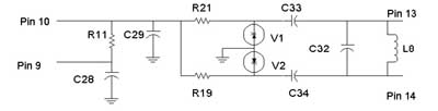
Note: This example is highly layout dependant and is based on the TRF6900EVM.
Q: How can I increase the current at PD_1 output?
A: Change the Rbias resistor connected to PD_SET (pin 8) to 75K ohms. This will increase the phase detector current to 100 uA, which in turn increases the phase detector gain to allow more PLL bandwidth.
Q: Can we extend the transmission distance by placing an amplifier circuit after your IC amplifier and before the transmit antenna.
A: Yes, you can put an external power amplifier between the TRF6900 and the antenna. You can use either a single Tx/Rx antenna port or else you can use a duplexor (ie. Murata LMS33L0897H002, Alpha AS157, AS169, etc.)
Q: If the TRF4900 chip is operated open-loop using fixed capacitors (no varactors) it appears that the output frequency drifts significantly (about 10 MHz) over time. The EVK compensates for this drift by using a very wide tuning range varactor arrangement. Can you please tell me where this drift is coming from and if it can be avoided?
A: The drift is due to the high impedance design and internal capacitors that charge up PIN4 and PIN5. The increased voltage shifts the VCO transistor working point and hence changes the parasitic capacities. To overcome the drift problem it is recommend to use a 100k ohm resistor - or higher - from PIN5 or PIN4 ( TRF4900) to ground to discharge the internal VCO capacitors.
Q: I am having problems in obtaining the varactors that TI has recommended for our design. Can you please suggest some additional varactor companies and part numbers?
A: Some alternative varactor diodes for the SMVxx that TI has not tested yet but theoretically should fit without major "redesign" of the VCO circuit are:
BBY51 or BBY52 from Infineon
http://www.infineon.com/cgi/ecrm.dll/ecrm/scripts/parameter_overview.jsp?oid=13803
or
BB154 should work also
http://www.semiconductors.com/handbook/chapter_902.html
Receiver Section:
Q: What is the sensitivity of the receiver?
A: We achieve, using the current material, (TRF6900 with high a mixer noise figure ) on our EVK at 38.4kBit/s a sensitivity of about -96dBm with a S/N of 14dB at the LNA input (for the TRF6900A we measure -105dBm). In general, the sensitivity must be calculated by the customer based on the chosen system architecture.
Q: In order to reduce component count only one IF-BPF ceramic filter is being used (only the 2nd IF amplifier/limiter), Will this degrade the receiver sensitivity or only selectivity
A: You will loose range due to selectivity, bit errors could increase, and the bitrate will decrease.
Q: How can we change the bandwidth of the discriminator? We want to use the TRF6900 for receiving FSK paging signals with a deviation of 5 kHz.
A: The bandwidth of the FM demodulator is determined by the Q of the external tank circuit. See spec. page 29 => L7, C16, C17, R28. The higher the Q the narrower the FM demodulation bandwidth. To narrow the bandwidth, increase or remove R28 and use a higher Q inductor. To widen the bandwidth reduce R28 and/or use a lower Q inductor. An extremely narrow FM demodulation bandwidth could require an FM tank adjustment during production.
Q: Is the mixer an image-reject mixer? If not, what do you do about the image frequency?
A: The mixer is not an image-reject mixer. For the 915MHz US ISM band it is necessary to use a filter to attenuate the image frequency. Alternatively the customer could use only a part of the 26MHz wide ISM band with a customized input filter. Due to the CT2+, GSM and TETRA services operation close to the 868 - 870MHz band the customers are forced to use SAW input filters. Therefore, in Europe the customers usually do not need an additional image suppression filter as the whole ISM band is only 2MHz wide and there are good (bandwidth 2MHz to 600kHz) input filters available with an image suppression of more than 50dB in the UHF signal path. Furthermore an additional filter would degrade the system sensitivity and increase the system costs and complexity.
Q: Can the TRF6900 resolve collisions when in the receive mode?
A: The TRF6900 is NOT a single frequency device. There is a fully programmable synthesizer on chip. The TRF6900 is able to operate in a "multi channel system" (FHSS system) as is often used in the US 915MHz ISM band. The TRF6900 has no "collision detection", this must be added externally.
Q: Can TI please recommend some SAW filters to be used with our design?
A:
| Mfg. |
P/N |
Bandwidth |
| Fujitsu |
FAR-F5CC-915M00-L2JZ |
(902 to 928 MHz) |
| MuRata |
SAFC915MA70N-TC11 |
|
| Sanyo |
TSM915AW-6 |
|
| Epcos |
B4637 |
|
MuRata also has narrower bandwidths available if required. This all depends on the number of channels needed in a given bandwidth & how close your channel spacing is.
| MuRata |
SAF903MF10T |
(902 to 904 MHz) |
| |
SAF915MA10N |
(913 to 917 MHz) |
| |
SAF927MF10T |
(926 to 928 MHz) |
Note that Epcos and Fujitsu also offer the narrow band filters as well.
General:
For general layout questions please consult the TRF6900 Application Report SWRA033.
Listed below are general RF layout guidelines for the TRF6900 (from most important to least important) based on the schematics in the datasheet.
- place PA output inductor L1 as close as possible to the chip
- place PA VCC capacitor C5 as close as possible to inductor L1
- place VCO tank inductor L8 as close as possible to the chip,
keep signal lines symmetrical
- place VCO tank capacitors C23 & C24 as close as possible to
inductor L8, keep signal lines symmetrical
- place LNA_IN inductor L2 as close as possible to the chip
- good grounding in the VCO area, PA area, LNA input & output
area, and under crystal circuit
- place LNA_VCC DC blocking capacitor C8 as close as
possible to the chip
- place DEMOD inductor L7 as close as possible to the chip
FYI: the LNA_IN and PA_OUT lines have been matched to 50 ohms on TI's EVMs.
Q: How critical is the positioning of BPF1 and BPF2 on the layout.
A: Repositioning BPF1 and/or BPF2 is not a problem.
Q: Can I rotate the crystal by 90 degrees with the ground tab away from the RF section. The same question applies for the antenna connection from above.
A: Repositioning the crystal is not a problem, just try to keep the XOSC1 (pin 23) and XOSC2 (pin 24) lines symmetrical.
Q: I am not able to find any 8.2nH, High Q, inductors for L2 and L8. I have been told that there are some 10nH inductors available, and I would like to know if that is an option?
Can we go with 10nH instead of 8.2nH for L2 and L8, or will this compromise the design?
A: Using a 10nH for both L2 and L8 is OK. In fact, we began our EVM builds using 10nH for both L2 and L8. Just make sure that L8 has a Q of 60 or greater.
Q: I wanted to ask if the filter, BPF2, on Figure 28 of the TRF6900 datasheet could be replaced with a zero-ohm resistor. The filter is not available, and so we were wondering if we would be able to get away with using a zero-ohm resistor in its place.
A: It's probably better to keep BPF2 and replace BPF1 with a 0.1uF capacitor which we do on all our TRF6900 EVMs. You should see minimal loss in range and sensitivity.
Q: We have found an available Murata filter (SFECV10.7MA5S-A-TC) having a 3db BW from fn of 280kHz +/- 50kHz. This is different than the 150 +/- 30kHz spec'd out in the transceiver data-sheet. My initial thought is that this wider bandwidth would mean more potential noise being received by the transceiver. Do you think that we would be able to use this filter?
A: Using a 280 kHz IF filter will create alot more problems, one being allowing in more potential noise as you mention below. Please use an IF filter between 100-150KHz and you should be OK.
Miscellaneous:
Q: What specifications have been found to be best for the crystal?
A:
| Frequency |
25.6 MHz. Or 26.0 MHz |
| Tolerance(+/- PPM)= |
20@25C |
| Stability(PPM)= |
20 @-4- to +85C |
| Load Capacitance� |
20pF |
| Max Series Resistance= |
40 ohms |
| Shunt Capacitance� |
5pF |
| Drive Level= |
.5 mW |
| Aging (PPM/Year)= |
6 |
Q: Can several IF filter part numbers be supplied so that I can choose the most available one for my application?
A: MuRata part numbers for surface mount 10.7 MHz IF filters are as follows:
| BW |
Part Number |
| 110 KHz |
SFECV10.7MHS-A-TC |
| 150 KHz |
MJS-A-TC |
| 180 kHz |
MS3S-A-TC |
| 230 kHz |
MS2S-A-TC |
| 280 kHz |
MA5S-A-TC |
| 330 kHz |
SFECV10.7MA2S-A-TC |
Note, filter center frequency accuracy at 10.7 MHz for the above list is +/- 30 kHz. Filter input/output impedance is 330 ohms.
Q: Can the TRF6900 operate at 370MHz?
A: The TRF6900 operates down to 350MHz (and probably lower); TI made some tests with the VCO, PA, LNA and Mixer. All blocks seemed to work well down to 350MHz, however, the TRF6900 is not specified or guaranteed to work at frequencies other than those in the datasheet.
Note: To operate on 350MHz you have to change the proposed VCO Tank circuit. The tuning range of the DDS or the reference frequency is no problem.
Q: I have Windows NT, can the MSP-EVKTRF6900 software run on my computer.
A No.
Q: Is it possible to realize a link in 868Mhz with 10 channels between 868.0 and 868.6 with a bandwidth of 50kHz and 50dB of protection between the two adjacent channels. The bitrate is 10K bit/s.
A: The system requirements of the TRF6900 fit exactly. 50dB of "protection" will be necessary therefore, a good IF filter is necessary. Keep in mind that 50dB is not easy to achieve with two 10.7MHz ceramic filters. There are 26kHz wide 10.7MHz ceramic filters on the market from Murata. However, if insufficient co-channel suppression is achieved use 21.4MHz or 10.7MHz crystal filters.
Q: Can you please explain the DEV bits? The D-word register shows the DEV to be bits {20:13}, i.e. 8-bits. The datasheet on page 20 shows the DEV to be Bits {9:2}, again 8 bit, but at a different location. The text then states that "the last two LSB's are set to zero; which agrees with {9:2}, but not with the D-word register.
A: The picture on page 20 shows where the 8 programmable bits are located inside the 24 bit DDS frequency register - it has nothing to do with the D-word of the serial control interface.
For example:
If we would align the 8 deviation bits at position 0 (LSB of the DDS frequency settings register) we would get a minimum frequency deviation of about 270Hz (+/-137Hz) and limit the maximum deviation to +/-35kHz. The maximum deviation is to low for wideband systems and of course nobody needs such a low minimum FSK deviation. Therefore, we shifted the 8 deviation bits left two times to get a minimum FSK deviation of about 1080Hz and a maximum deviation of +/-138kHz. Quite a good range by still programming only 8 bits. The position of the 8 FSK deviation bits inside the D-word is still 20:13.
Q: I believe that the TRF6900 transmit/receive frequencies are software programmable but if the frequencies vary widely then the S/W programmable bits as well as the external components (resistors, caps, and maybe inductors) would need to be changed. Is this correct?
A: The operating frequency range is determined by the VCO circuit. Within the tuning range of the VCO, reprogramming the device can change the frequency. To optimize the performance you have to change some the external components in order to optimize the matching of the LNA, Mixer etc. on the chosen frequency range.
Q: What ranges are the TRF6900 & TRF6900A devices capable of?
A: 100-200 yards is what several customers get, one has seen more than 200 yards outdoors. 300 yards should be do-able. This is the theoretical calculation for a direct wave along flat terrain (no hills, mountains, buildings etc.) with a Tx @ +5 dBm (or approx 3 mw) and a Rx sensitivity of -85 dBm, with an antenna gain = 0 dBm, the transmission distance is as follows:
Pt - Pr = +5 dBm - (-85 dbm)
        = 90 dBm
Path Loss = 37 + 20 Log "f" (MHz) + 20 Log "d" (miles)
90        = 37 + 20 Log 915 + 20 Log "d"
          = 37 + 59.2 + 20 Log "d"
          = 96.2 + 20 Log "d"
90 - 96.2 = 20 Log "d"
    - 6.2 = 20 Log "d"
   6.2/20 = Log "d"
 - 0.3114 = Log "d"
10^ (-.3114) = "d"
0.4881788 = "d" Hence we can transmit 0.488 miles, or
1 mile = 5,280 feet therefore, distance in feet =
0.4881788 * 5,280 = 2,577 feet
|