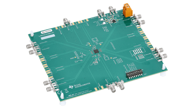
Features for the LMK00338EVM
- Low-noise clock fan-out with two banks of four HCSL outputs each and one LVCMOS output
- 3:1 input multiplexer with two universal input buffers and one crystal oscillator interface, selectable via control pins
- Includes DIP switches to configure control pins
- 3.3 V core and independent 3.3 V/2.5 V output supplies per output bank using onboard regulator options or direct supply inputs
- Flexible input/output interface with controlled-impedance traces and edge SMA connectors
Description for the LMK00338EVM
The LMK00338 is a 400MHz, 8-output HCSL buffer intended for PCIe Gen1/2/3 Applications, low additive jitter clock distribution and level translation. The EVM allows the user to verify the functionality and performance specification of the device. Refer to the LMK00338 datasheet for the functional description and specifications.