SNAS308G April 2005 – May 2016 ADC081S021
PRODUCTION DATA.
- 1 Features
- 2 Applications
- 3 Description
- 4 Revision History
- 5 Device Comparison Table
- 6 Pin Configuration and Functions
- 7 Specifications
- 8 Detailed Description
- 9 Application and Implementation
- 10Power Supply Recommendations
- 11Layout
- 12Device and Documentation Support
- 13Mechanical, Packaging, and Orderable Information
Package Options
Mechanical Data (Package|Pins)
Thermal pad, mechanical data (Package|Pins)
Orderable Information
8 Detailed Description
8.1 Overview
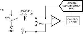
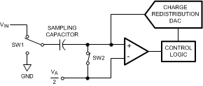
The ADC081S021 is a successive-approximation analog-to-digital converter designed around a charge-redistribution digital-to-analog converter core. Simplified schematics of the ADC081S021 in both track and hold modes are shown in Figure 19 and Figure 18, respectively. In Figure 19, the device is in track mode: switch SW1 connects the sampling capacitor to the input, and SW2 balances the comparator inputs. The device is in this state until CS is brought low, at which point the device moves to hold mode.
8.2 Functional Block Diagram

8.3 Feature Description
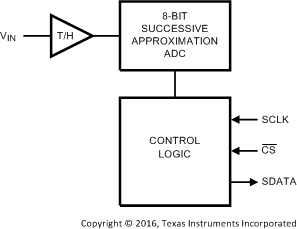
The serial interface timing diagram for the ADC is shown in Timing Requirements. CS is chip select, which initiates conversions on the ADC and frames the serial data transfers. SCLK (serial clock) controls both the conversion process and the timing of serial data. SDATA is the serial data out pin, where a conversion result is found as a serial data stream.
Basic operation of the ADC begins with CS going low, which initiates a conversion process and data transfer. Subsequent rising and falling edges of SCLK are labelled with reference to the falling edge of CS; for example, the third falling edge of SCLK shall refer to the third falling edge of SCLK after CS goes low.
At the fall of CS, the SDATA pin comes out of TRI-STATE and the converter moves from track mode to hold mode. The input signal is sampled and held for conversion on the falling edge of CS. The converter moves from hold mode to track mode on the 13th rising edge of SCLK (see Timing Requirements). It is at this point that the interval for the TACQ specification begins. At least 350 ns must pass between the 13th rising edge of SCLK and the next falling edge of CS. The SDATA pin is placed back into TRI-STATE after the 16th falling edge of SCLK, or at the rising edge of CS, whichever occurs first. After a conversion is completed, the quiet time (tQUIET) must be satisfied before bringing CS low again to begin another conversion.
Sixteen SCLK cycles are required to read a complete sample from the ADC. The sample bits (including leading or trailing zeroes) are clocked out on falling edges of SCLK, and are intended to be clocked in by a receiver on subsequent rising edges of SCLK. The ADC produces three leading zero bits on SDATA, followed by eight data bits, most significant first. After the data bits, the ADC clocks out four trailing zeros.
If CS goes low before the rising edge of SCLK, an additional (fourth) zero bit may be captured by the next falling edge of SCLK.
8.3.1 Determining Throughput
Throughput depends on the frequency of SCLK and how much time is allowed to elapse between the end of one conversion and the start of another. At the maximum specified SCLK frequency, the maximum ensured throughput is obtained by using a 20 SCLK frame. As shown in Timing Requirements, the minimum allowed time between CS falling edges is determined by:
- 12.5 SCLKs for Hold mode.
- The larger of two quantities: either the minimum required time for Track mode (tACQ) or 2.5 SCLKs to finish reading the result.
- 0, 1/2, or 1 SCLK padding to ensure an even number of SCLK cycles so there is a falling SCLK edge when CS next falls.
(12.5 SCLKs + tACQ + 1/2 SCLK) which corresponds to a maximum throughput of 1 MSPS. At the slowest rate for this family, SCLK is 1 MHz. Using a 20 cycle conversion frame as shown in Timing Requirements yields a 20-μs time between CS falling edges for a throughput of 50 KSPS. It is possible, however, to use fewer than 20 clock cycles provided the timing parameters are met. With a 1-MHz SCLK, there are 2500 ns in 2.5 SCLK cycles, which is greater than tACQ. After the last data bit has come out, the clock needs one full cycle to return to a falling edge. Thus the total time between falling edges of CS is 12.5 × 1 μs + 2.5 × 1 μs + 1 × 1 μs = 16 μs which is a throughput of 62.5 KSPS.
8.4 Device Functional Modes
Figure 18 shows the device in hold mode: switch SW1 connects the sampling capacitor to ground, maintaining the sampled voltage, and switch SW2 unbalances the comparator. The control logic then instructs the charge-redistribution DAC to add or subtract fixed amounts of charge from the sampling capacitor until the comparator is balanced. When the comparator is balanced, the digital word supplied to the DAC is the digital representation of the analog input voltage. The device moves from hold mode to track mode (Figure 19) on the 13th rising edge of SCLK.
 Figure 18. Hold Mode
 Figure 19. Track Mode
8.4.1 Transfer Function
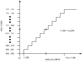
The output format of the ADC is straight binary. Code transitions occur midway between successive integer LSB values. The LSB width for the ADC is VA/256. The ideal transfer characteristic is shown in Figure 20. The transition from an output code of 0000 0000 to a code of 0000 0001 is at 1/2 LSB, or a voltage of VA/512. Other code transitions occur at steps of one LSB.
 Figure 20. Ideal Transfer Characteristic
8.4.2 Modes of Operation
The ADC has two possible modes of operation: normal mode and shutdown mode. The ADC enters normal mode (and a conversion process is begun) when CS is pulled low. The device enters shutdown mode if CS is pulled high before the tenth falling edge of SCLK after CS is pulled low, or stays in normal mode if CS remains low. Once in shutdown mode, the device stays there until CS is brought low again. By varying the ratio of time spent in the normal and shutdown modes, a system may trade off throughput for power consumption, with a sample rate as low as zero.
8.4.2.1 Normal Mode
The fastest possible throughput is obtained by leaving the ADC in normal mode at all times, so there are no power-up delays. To keep the device in normal mode continuously, CS must be kept low until after the 10th falling edge of SCLK after the start of a conversion (remember that a conversion is initiated by bringing CS low).
If CS is brought high after the 10th falling edge, but before the 16th falling edge, the device remains in normal mode, but the current conversion is aborted and the SDATA returns to TRI-STATE (truncating the output word).
Sixteen SCLK cycles are required to read all of a conversion word from the device. After sixteen SCLK cycles have elapsed, CS may be idled either high or low until the next conversion. If CS is idled low, it must be brought high again before the start of the next conversion, which begins when CS is again brought low.
After sixteen SCLK cycles, SDATA returns to TRI-STATE. Another conversion may be started, after tQUIET has elapsed, by bringing CS low again.
8.4.2.2 Shutdown Mode
Shutdown mode is appropriate for applications that either do not sample continuously, or it is acceptable to trade throughput for power consumption. When the ADC is in shutdown mode, all of the analog circuitry is turned off.
To enter shutdown mode, a conversion must be interrupted by bringing CS high anytime between the second and tenth falling edges of SCLK, as shown in Figure 21. Once CS has been brought high in this manner, the device enters shutdown mode, the current conversion is aborted and SDATA enters TRI-STATE. If CS is brought high before the second falling edge of SCLK, the device does not change mode; this is to avoid accidentally changing mode as a result of noise on the CS line.
 Figure 21. Entering Shutdown Mode
 Figure 22. Entering Normal Mode
To exit shutdown mode, bring CS back low. Upon bringing CS low, the ADC begins powering up (power-up time is specified in Timing Requirements). This microsecond of power-up delay results in the first conversion result being unusable. The second conversion performed after power up, however, is valid, as shown in Figure 22.
If CS is brought back high before the 10th falling edge of SCLK, the device returns to shutdown mode. This is done to avoid accidentally entering normal mode as a result of noise on the CS line. To exit shutdown mode and remain in normal mode, CS must be kept low until after the 10th falling edge of SCLK. The ADC is fully powered up after 16 SCLK cycles.