SBAS672E July 2014 – June 2022 ADC3221 , ADC3222 , ADC3223 , ADC3224
PRODUCTION DATA
- 1 Features
- 2 Applications
- 3 Description
- 4 Revision History
- 5 Pin Configuration and Functions
-
6 Specifications
- 6.1 Absolute Maximum Ratings
- 6.2 ESD Ratings
- 6.3 Recommended Operating Conditions (1)
- 6.4 Thermal Information
- 6.5 Electrical Characteristics: General
- 6.6 Electrical Characteristics: ADC3221, ADC3222
- 6.7 Electrical Characteristics: ADC3223, ADC3224
- 6.8 AC Performance: ADC3221
- 6.9 AC Performance: ADC3222
- 6.10 AC Performance: ADC3223
- 6.11 AC Performance: ADC3224
- 6.12 Digital Characteristics
- 6.13 Timing Requirements: General
- 6.14 Timing Requirements: LVDS Output
- 6.15 Typical Characteristics: ADC3221
- 6.16 Typical Characteristics: ADC3222
- 6.17 Typical Characteristics: ADC3223
- 6.18 Typical Characteristics: ADC3224
- 6.19 Typical Characteristics: Common
- 6.20 Typical Characteristics: Contour
- 7 Parameter Measurement Information
-
8 Detailed Description
- 8.1 Overview
- 8.2 Functional Block Diagram
- 8.3 Feature Description
- 8.4 Device Functional Modes
- 8.5 Programming
- 8.6
Register Maps
- 8.6.1 Summary of Special Mode Registers
- 8.6.2
Serial Register Description
- 8.6.2.1 Register 01h
- 8.6.2.2 Register 03h
- 8.6.2.3 Register 04h
- 8.6.2.4 Register 05h
- 8.6.2.5 Register 06h
- 8.6.2.6 Register 07h
- 8.6.2.7 Register 09h
- 8.6.2.8 Register 0Ah
- 8.6.2.9 Register 0Bh
- 8.6.2.10 Register 0Eh
- 8.6.2.11 Register 0Fh
- 8.6.2.12 Register 13h
- 8.6.2.13 Register 15h
- 8.6.2.14 Register 25h
- 8.6.2.15 Register 27h
- 8.6.2.16 Register 41Dh
- 8.6.2.17 Register 422h
- 8.6.2.18 Register 434h
- 8.6.2.19 Register 439h
- 8.6.2.20 Register 51Dh
- 8.6.2.21 Register 522h
- 8.6.2.22 Register 534h
- 8.6.2.23 Register 539h
- 8.6.2.24 Register 608h
- 8.6.2.25 Register 70Ah
- 9 Applications and Implementation
- 10Device and Documentation Support
- 11Mechanical, Packaging, and Orderable Information
Package Options
Mechanical Data (Package|Pins)
- RGZ|48
Thermal pad, mechanical data (Package|Pins)
- RGZ|48
Orderable Information
3 Description
The ADC322x are a high-linearity, ultra-low power, dual-channel, 12-bit, 25-MSPS to 125-MSPS, analog-to-digital converter (ADC) family. The devices are designed specifically to support demanding, high input frequency signals with large dynamic range requirements. An input clock divider allows more flexibility for system clock architecture design and the SYSREF input enables complete system synchronization. The ADC322x family supports serial low-voltage differential signaling (LVDS) in order to reduce the number of interface lines, thus allowing for high system integration density. The serial LVDS interface is two-wire, where each ADC data are serialized and output over two LVDS pairs. Optionally, a one-wire serial LVDS interface is available. An internal phase-locked loop (PLL) multiplies the incoming ADC sampling clock to derive the bit clock that is used to serialize the 12-bit output data from each channel. In addition to the serial data streams, the frame and bit clocks are also transmitted as LVDS outputs.
| PART NUMBER | PACKAGE(1) | BODY SIZE (NOM) |
|---|---|---|
| ADC322x | VQFN (48) | 7.00 mm × 7.00 mm |
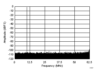
 Performance at fS = 125 MSPS, fIN = 10 MHz (SNR = 70.6
dBFS, SFDR = 100 dBc)