SBAS656B September 2015 – April 2016 ADS1257
PRODUCTION DATA.
- 1 Features
- 2 Applications
- 3 Description
- 4 Revision History
- 5 Device Comparison Table
- 6 Pin Configuration and Functions
-
7 Specifications
- 7.1 Absolute Maximum Ratings
- 7.2 ESD Ratings
- 7.3 Recommended Operating Conditions
- 7.4 Thermal Information
- 7.5 Electrical Characteristics
- 7.6 Serial Interface Timing Requirements
- 7.7 Serial Interface Switching Characteristics
- 7.8 RESET and SYNC/PWDN Timing Requirements
- 7.9 SCLK Reset Timing Requirements
- 7.10 DRDY Update Timing Characteristics
- 7.11 Typical Characteristics
- 8 Parameter Measurement Information
-
9 Detailed Description
- 9.1 Overview
- 9.2 Functional Block Diagram
- 9.3
Feature Description
- 9.3.1 Input Multiplexer
- 9.3.2 Analog Input Buffer
- 9.3.3 Programmable Gain Amplifier (PGA)
- 9.3.4 Modulator Input Circuitry
- 9.3.5 Voltage Reference Inputs (REFP, REFN)
- 9.3.6 Clock Input (CLKIN)
- 9.3.7 Clock Output (D0/CLKOUT)
- 9.3.8 General-Purpose Digital I/O (D0, D1)
- 9.3.9 Open- and Short-Circuit Sensor Detection
- 9.3.10 Digital Filter
- 9.4 Device Functional Modes
- 9.5
Programming
- 9.5.1 Serial Interface
- 9.5.2 Data Format
- 9.5.3
Command Definitions
- 9.5.3.1 WAKEUP/NOP: Complete Synchronization or Exit Standby Mode
- 9.5.3.2 RDATA: Read Data
- 9.5.3.3 RDATAC: Read Data Continuous
- 9.5.3.4 SDATAC: Stop Read Data Continuous
- 9.5.3.5 RREG: Read from Registers
- 9.5.3.6 WREG: Write to Register
- 9.5.3.7 SELFCAL: Self-Offset and Self-Gain Calibration
- 9.5.3.8 SELFOCAL: Self Offset Calibration
- 9.5.3.9 SELFGCAL: Self Gain Calibration
- 9.5.3.10 SYSOCAL: System Offset Calibration
- 9.5.3.11 SYSGCAL: System Gain Calibration
- 9.5.3.12 STANDBY: Standby Mode / Single-shot Mode
- 9.5.3.13 RESET: Reset Registers to Default Values
- 9.5.3.14 SYNC: Synchronize the Analog-to-Digital Conversion
- 9.6
Register Map
- 9.6.1 STATUS: Status Register (address = 00h) [reset = x1h]
- 9.6.2 MUX : Input Multiplexer Control Register (address = 01h) [reset = 01h]
- 9.6.3 ADCON: ADC Control Register (address = 02h) [reset = 20h]
- 9.6.4 DRATE: ADC Data Rate Register (address = 03h) [reset = F0h]
- 9.6.5 IO: GPIO Control Register (address = 04h) [reset = E0h]
- 9.6.6 OFC0: Offset Calibration Register 0 (address = 05h) [reset = depends on calibration results]
- 9.6.7 OFC1: Offset Calibration Register 1 (address = 06h) [reset = depends on calibration results]
- 9.6.8 OFC2: Offset Calibration Register 2 (address = 07h) [reset = depends on calibration results]
- 9.6.9 FSC0: Full-Scale Calibration Register 0 (address = 08h) [reset = depends on calibration results]
- 9.6.10 FSC1: Full-Scale Calibration Register 1 (address = 09h) [reset = depends on calibration results]
- 9.6.11 FSC2: Full-Scale Calibration Register 2 (address = 0Ah) [reset = depends on calibration results]
- 10Applications and Implementation
- 11Power Supply Recommendations
- 12Layout
- 13Device and Documentation Support
- 14Mechanical, Packaging, and Orderable Information
Package Options
Mechanical Data (Package|Pins)
- RGW|20
Thermal pad, mechanical data (Package|Pins)
- RGW|20
Orderable Information
10 Applications and Implementation
NOTE
Information in the following applications sections is not part of the TI component specification, and TI does not warrant its accuracy or completeness. TI’s customers are responsible for determining suitability of components for their purposes. Customers should validate and test their design implementation to confirm system functionality.
10.1 Application Information
The ADS1257 is a precision, 24-bit, ΔΣ ADC. Optimal performance is achieved with the ADS1257 by careful attention to the design of supporting circuitry and the printed circuit board (PCB) layout, as discussed in the following sections.
10.1.1 Basic Connections
Figure 60 shows the principle connections for the ADS1257.
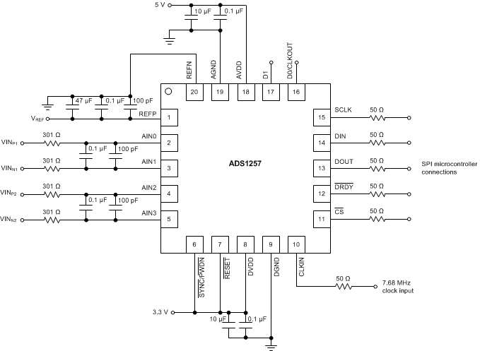 Figure 60. ADS1257 Basic Connections
10.1.2 Digital Interface Connections
The ADS1257 5-V tolerant SPI-, QSPI™-, and Microwire™-compatible serial interface connects to a wide variety of microcontroller SPI peripherals. The interface operates in SPI mode 1, where CPOL = 0 and CPHA = 1. In SPI mode 1, SCLK idles low and data are updated only on SCLK rising edges; data are latched or read by the ADC and external controller on SCLK falling edges. See the Serial Interface Timing Requirements for details of the SPI communication protocol employed by the device.
Figure 61 shows how to connect to microcontrollers with a dedicated SPI, such as TI’s MSP430 family of low-power microcontrollers. Additionally, the ADS1257 can connect to an 8xC51 UART in a two-wire configuration using serial mode 0, as shown in Figure 62. Avoid using read-data-continuous mode (RDATAC) when DIN and DOUT are connected together.
Place small series resistors on all digital signals to help smooth sharp transitions, suppress overshoot, and provide some overvoltage protection. Additional delays (due to the added resistance and bus capacitance) must still meet the SPI timing requirements.
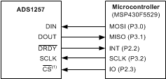
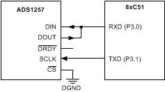 Figure 62. Connection to 8xC51 Microcontroller UART With a 2-Wire Interface
10.1.3 Analog Input Filtering
Analog input filtering serves two purposes:
- To limit the effect of aliasing during the sampling process.
- To reduce the amount of external noise in the measurement.
As with any sampled system, aliasing can occur if proper antialias filtering is not in place. Aliasing occurs when frequency components are present in the input signal that are higher than half the sampling frequency of the ADC (also known as the Nyquist frequency). These frequency components are folded back into the frequency band of interest below half the sampling frequency. Inside a delta-sigma (ΔΣ) ADC, however, the input signal is sampled at the modulator frequency f(MOD) and not at the output data rate. The filter response of the digital filter repeats at multiples of the sampling frequency (f(MOD)), as shown in Figure 63. Signals or noise up to frequencies near f(MOD) are attenuated to a certain amount by the digital filter. Any frequency components present in the input signal around the modulator frequency, or multiples thereof, are not attenuated and alias back into the band of interest unless attenuated by an external analog filter.
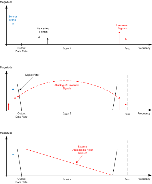 Figure 63. Alias Effect
Many sensor signals are inherently band-limited; for example, the output of a thermocouple has a limited rate of change. When band-limited, the sensor signal does not alias back into the pass band when using a ΔΣ ADC. However, any noise pick-up along the sensor wiring or the application circuitry can potentially alias into the pass-band. Power line-cycle frequency and harmonics are one common noise source example. External noise can also be generated from electromagnetic interference (EMI) or radio frequency interference (RFI) sources, such as nearby motors and cellular phones. Another noise source exists on the printed circuit board (PCB) itself in the form of clocks and other digital signals. Analog input filtering may help prevent such unwanted signals from affecting the measurement result.
A first-order resistor-capacitor (RC) filter is usually sufficient to either totally eliminate aliasing, or to reduce the effect of aliasing to a level within the noise floor of the sensor. Ideally, any signal beyond f(MOD) / 2 is attenuated to a level below the noise floor of the ADC. The digital filter of the ADS1257 attenuates signals to a certain degree, as illustrated in the filter response plots in the Digital Filter section. In addition, noise components are usually smaller in magnitude than the actual sensor signal. Therefore, using a first-order RC filter with a cutoff frequency set at the output data rate or higher is generally a good starting point for a system design. Avoid capacitors with low-grade dielectrics to minimize temperature variations and leakage.
10.1.4 External Reference
ADC measurement results are proportional to the ratio of the input and reference voltages; therefore, a stable and low-noise reference source is required for stable results. Select a reference source that is low noise, low drift, and low output impedance (such as the REF5025), which can drive the ADS1257 reference inputs directly. For voltage references not suited for driving the ADS1257 reference inputs directly (for example, high output impedance references or resistive voltage dividers), use the buffer circuit shown in Figure 64.
 Figure 64. Voltage Reference Buffer Circuit
Always use low equivalent series resistance (ESR) capacitors to bypass the voltage reference signal near the ADS1257 reference input pins (REFP and REFN). Make these capacitors large in order to increase the filtering on the reference. Larger reference capacitors may take additional time to settle after power-up and when starting conversions.
The reference voltage (VREF) must be between 0.5 V and 2.6 V.
10.1.5 Isolated (or Floating) Sensor Inputs
Isolated sensors (sensors that are not referenced to the ADC ground) must have an established common-mode voltage within the ADCs absolute input range, as specified by the Recommended Operating Conditions. Bias the ADCs input common-mode voltage by external resistors or by connecting to a dc voltage, such as the external reference voltage.
10.1.6 Unused Inputs and Outputs
To minimize leakage currents on the analog inputs, leave unused analog inputs floating, connect them to midsupply, or connect them to AVDD. Unused analog inputs can also be connected to AVSS, but may yield higher leakage currents than other connection options.
Tie all unused digital inputs to the appropriate levels (DVDD or DGND), including when in power-down mode. Do not float the digital inputs to the ADC; excessive power-supply leakage current can result. The D0/CLKOUT and D1 pins can be left floating if configured as outputs. If the DRDY output is not used, leave the DRDY pin unconnected or tie the pin to DVDD using a weak pull-up resistor.
10.1.7 Pseudo Code Example
The following list shows a sequence of steps for device set-up. The DRDY pin is used to indicate new conversion data. The register settings are configured for input buffer enabled, PGA gain = 16 V/V, and a data rate of 10 SPS.
Power-up the analog and digital supplies (allow time for power supplies to settle);

Set microcontroller GPIOs connected to the RESET and SYNC/PWDN pins low;
Configure the SPI of the microcontroller to SPI mode 1 (CPOL = 0, CPHA =1);
If the CS pin is not tied low permanently, configure microcontroller GPIO connected to CS as an output;
Configure microcontroller GPIO connected to the DRDY pin as a falling-edge triggered interrupt input;
Enable the external clock driving the CLKIN pin;
Enable the device by setting the RESET and SYNC/PWDN pins high;
Wait a minimum of 8192 clock cycles or for DRDY to transition low;

Set CS to the device low;
Delay for a minimum of t3;

Reset and Self-Calibration
{
	Send the RESET command (FEh) after power-up;
	Wait for DRDY to transition low (self-calibration has completed);
}

Send the SDATAC command (0Fh);
Delay for a minimum of t11;
Write the respective register configuration with the WREG command (50h, 03h, 02h, 01h, 24h and 23h);
Optional: As a sanity check, read back all configuration registers with the RREG command (10h);
Delay for a minimum of t11;

Send the RDATAC command (03h);
Delay for a minimum of t10;
Clear CS to high (resets the serial interface);

Loop
{
	Wait for DRDY to transition low;
	Take CS low;
	Delay for a minimum of t3;
	Send 24 SCLK rising edges to read out conversion data on DOUT;
	Delay for a minimum of t10;
	Clear CS to high;
}

Take SYNC/PWDN low for a minimum of 20 DRDY cycles to put the device in power-down mode;
10.2 Typical Application
Figure 65 shows an example of a programmable-logic controller (PLC) analog front-end circuit with ±10 V and 4-20 mA inputs, with 10% input over-range tolerance. A level-shifted resistor divider (R1 and R2) accepts input voltages from –11 V to +11 V, and a ground-referenced current-sense resistor (R3) allows for current inputs ranging from 0 to 22 mA. The ADS1257 does not require any additional signal conditioning with its integrated multiplexer, buffer, PGA, and four analog input pins that accept single-ended, AGND-referenced voltages. The REF5025 provides the ADC reference voltage, and is capable of driving the ADC reference input pins without additional buffering. Resistor divider R4 and R5 and the buffer amplifier (OPA188) provide a 1.5-V level shift for the ±10-V input divider network. All three devices (the ADS1257, REF5025, and OPA188) are powered by a single 5-V supply.
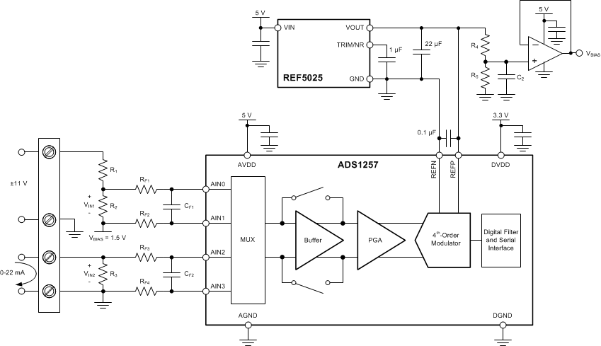 Figure 65. ±10-V and 4-20-mA Inputs for Programmable Logic Controller (PLC) Module
10.2.1 Design Requirements
Table 28. Design Requirements
| DESIGN PARAMETER | VALUE |
|---|---|
| Supply voltages | 5.0-V analog (unipolar) and 3.3-V digital |
| Data rate | 10 SPS (simulataneous 50 / 60 Hz rejection) |
| Voltage input | ±10 V (±10% overrange)(1)
Input impedance ≥ 200 kΩ |
| Current input | 4 mA to 20 mA (±10% overrange)(2) |
| Calibrated accuracy at TA = 25°C | ±0.01% |
10.2.2 Detailed Design Procedure
10.2.2.1 Detailed Design Procedure for ±10-V Input
The following sections discuss the design of the PLC voltage input circuitry.
10.2.2.1.1 Absolute Input Voltage Range
A resistor divider attenuates and level shifts a ±10-V input signal to within the ADC input range, to create a linear relationship between the input signal voltage and ADC output code. Before designing the input circuitry, the ADC absolute and differential input voltage ranges are considered.
The input range of the ADS1257 depends on the analog supply voltage, the reference voltage, the state of the internal buffer (enabled or disabled), and the PGA gain. Input voltages must be within the absolute input voltage range of the ADC. The largest absolute input voltage range is achieved when the internal buffer is disabled, allowing for input signals between AGND – 0.1 V and AVDD + 0.1 V. However, the ADC input impedance is low when the buffer is disabled, causing the ADC to load input signals that have a high source impedance and are not buffered. Enable the buffer to increase the ADC input impedance, and significantly reduce the loading on the input signal. When the internal buffer is enabled, the input signal range is limited to voltages between AGND and AVDD – 2 V.
In the circuit shown in Figure 65, the voltage divider uses large-value resistors to reduce loading of the transmitted signal; therefore, the ADS1257 internal buffer is enabled to significantly reduce loading on the resistor divider. As a result, input signals to the ADC are limited to voltages between 0 V to 3 V (AVDD = 5 V, buffer enabled). Therefore, a level-shifted, single-ended input signal allows for a bipolar signal with maximum amplitude of ±1.5 V. Some additional headroom may be required to allow for analog supply-voltage tolerance.
10.2.2.1.2 Differential Input Voltage Range
The input voltage (VIN1) must not exceed the differential input voltage range so that the ADC can provide an output code for every input voltage and avoid clipped output codes. The differential input voltage range is limited, in part by the absolute input voltage range, but also by the reference voltage and PGA gain. The differential input voltage range of the ADS1257 is given by Equation 5.
Using a nominal reference voltage of 2.5 V, the PGA gain is selected to allow for the largest input signal range and lowest ADC input-referred noise. The ratio of input signal to ADC noise is calculated as the number of noise-free bits, using Equation 6.
where
- VIN_PP is the peak-to-peak input signal voltage range
- VNOISE_RTI_PP is the peak-to-peak input-referred noise (VPP ≈ 6.6 · VRMS)
The maximum achievable noise-free bit resolution is calculated for various PGA gains as shown in Table 29.
Table 29. Voltage Resolution Comparison for Various PGA Gains
| PGA GAIN (V/V) | MAXIMUM DIFFERENTIAL INPUT VOLTAGE | INPUT-REFERRED NOISE AT 10 SPS (3) | NOISE-FREE BITS |
|---|---|---|---|
| 1 | ±1.5 V(1) | 2.24 µVPP | 20.4 |
| 2 | ±1.5 V(1) | 1.41 µVPP | 21.0 |
| 4 | ±1.25 V(2) | 0.91 µVPP | 21.4 |
| 8 | ±0.625 V(2) | 0.70 µVPP | 20.8 |
A PGA gain of 4 V/V is selected to achieve the highest voltage resolution; therefore, the differential input voltage must be limited to ±1.25 V to avoid overranging the ADC input. With the ADC differential input voltage range defined, the attenuation ratio of the resistor divider can be calculated.
10.2.2.1.3 Level-Shifted Resistor Divider Sizing
To attenuate the ±10-V signal (with 10% overrange) down to ±1.25 V, the resistor divider must have a gain less than 1.25 / 11 = 1 / 8.8 = 0.113 V/V. To achieve this attenuation, R1 must be ≥ 9.8 · R2. Additionally, the input impedance of the resistor divider (R1 + R2) must be ≥ 200 kΩ. Solving these requirements determines that R2 must be ≥ 22.73 kΩ. Standard resistor values of 24.9 kΩ for R2, and 200 kΩ for R1 are chosen to satisfy the design requirements. Larger resistor values can also be used, but result in increased resistor thermal noise. Resistor noise must not exceed the ADC input-referred noise, or resolution degrades. Additionally, select resistors R1 and R2 to have low temperature coefficients in order to reduce the gain error drift of the resistor divider.
To level-shift the input signal and satisfy the ADS1257 absolute input range, R2 is connected to a 1.5-V bias voltage. This bias voltage is derived from another resistor divider (R4 and R5) connected to the REF5025 output. Use values of 2 kΩ for R4, and 3 kΩ for R5 in order to provide the 1.5-V bias output. This voltage is buffered to avoid loading and provide a stable common-mode input voltage for the ADS1257.
Figure 66 and Figure 67 show the input transfer functions with respect to the ADC absolute and differential input voltage ranges, respectively.
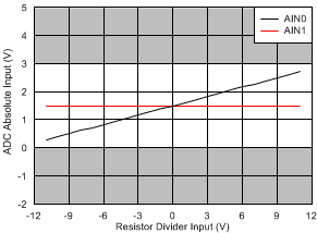
| AVDD = 5 V, buffer enabled |
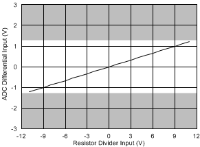
| VREF = 2.5 V, PGA = 4 V/V |
10.2.2.1.4 Input Filtering
The differential RC filters are chosen to set the –3-dB corner frequency to be 1000 times wider than the ADC digital filter bandwidth in order to allow for fast RC settling and common component values. The selected ADS1257 sampling rate of 10 SPS results in a –3-dB digital filter bandwidth of 4.4 Hz. The –3-dB filter corner frequency for the input RC filter is set to approximately 5 kHz. Analog input currents of the ADC cause a voltage drop across the filter resistors that results in an offset error if either the bias currents or filter resistors are not equal. These resistors are limited to several kΩ in order to reduce resistor thermal noise and dc offset errors due to input bias currents. These resistors also provide a certain amount of input fault protection in case of an input overvoltage event. RF1 and RF2 are chosen to be 1.5 kΩ. The input filter differential capacitor (CF1) is calculated from the selected cutoff frequency (f–3dB_DIFF), as shown in Equation 7.
After calculating the capacitance of CF1, the capacitor is chosen to be a standard value of 10 nF.
10.2.2.1.5 Register Settings for ±10-V Input
The register settings for the PLC voltage measurement are shown in Table 30.
Table 30. Register Settings for ±11-V Input
| REGISTER | NAME | SETTING | DESCRIPTION |
|---|---|---|---|
| 00h | STATUS | 0Ah | MSB first, buffer enabled |
| 01h | MUX | 01h | Select AIN0 = AINP and AIN1 = AINN |
| 02h | ADCON | 02h | CLKOUT OFF, sensor detect OFF, gain = 4 V/V |
| 03h | DRATE | 23h | Data rate = 10 SPS |
10.2.2.1.6 Voltage Input Design Variations
The level-shifted resistor divider is sized to allow for input signals up to ±10 V (with 10% overrange); however, different resistor values may be chosen to optimize the circuit for other common input voltage ranges, such as ±5 V, ±2.5 V, ±1 V, 0 V to 10 V, 0 V to 5 V, 0 V to 2.5 V, and 0 V to 1 V. For unipolar input ranges, remove the OPA188 and bias voltage resistor divider (R4 and R5) and connect the bias voltage (VBIAS) to AGND.
10.2.2.2 Detailed Design Procedure for 4-mA to 20-mA Input
The following sections discuss the design of the PLC current input circuitry.
10.2.2.2.1 PGA Gain Selection
The previous Absolute Input Voltage Range and Differential Input Voltage Range considerations for the PLC voltage input circuitry also apply to the 4-mA to 20-mA current input design. However, the current-sense resistor is not level-shifted and input signals to the ADC are limited to positive voltages between 0-3 V (for buffer enabled, PGA gain = 1 V/V). Therefore, the noise-free bit resolution is recalculted for the modified input signal range for various PGA gains, as shown in Table 31.
Table 31. Current Resolution Comparison for Various PGA Gains
| PGA GAIN (V/V) |
INPUT SIGNAL RANGE | INPUT-REFERRED NOISE AT 10 SPS(3) | NOISE-FREE BITS |
|---|---|---|---|
| 1 | 0 to 3 V(1) | 2.24 µVPP | 20.4 |
| 2 | 0 to 2.5 V(2) | 1.41 µVPP | 20.8 |
| 4 | 0 to 1.25 V(2) | 0.91 µVPP | 20.4 |
| 8 | 0 to 0.625 V(2) | 0.70 µVPP | 19.8 |
A PGA gain of 2 V/V is selected to achieve the highest input current resolution. Therefore, the differential input voltage is limited to voltages between 0 V and 2.5 V.
10.2.2.2.2 Current-Sense Resistor Sizing
To convert the 0-mA to 22-mA current into an input voltage between 0 V and 2.5 V, the current-sense resistor (R3) must be ≤ 113.6 Ω. A standard resistor value of 100 Ω with a low temperature coefficient is chosen for R3.
In addition to the resistance, make sure to consider the power dissipation. Resistor power dissipation (PD) is given by Equation 8.
For the maximum current of 22 mA, the R3 resistor dissipates 48.4 mW during normal operation. However, a larger power rating is required to accommodate temperature derating and input overvoltages. A low-leakage, transient-voltage-suppression (TVS) diode in parallel with R3 reduces the power dissipated by this resistor in case of an input overvoltage. Figure 68 and Figure 69 show the current input-transfer functions, with respect to the ADC absolute input range and differential input voltage range, respectively.
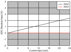
| AVDD = 5 V, buffer enabled |
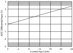
| VREF = 2.5 V, PGA = 4 V/V |
10.2.2.2.3 Register Settings for 4-mA to 20-mA Input
The register settings for the PLC current measurement are shown in Table 32.
Table 32. Register Settings for 4-mA to 20-mA Input
| REGISTER | NAME | SETTING | DESCRIPTION |
|---|---|---|---|
| 00h | STATUS | 0Ah | MSB first, buffer enabled |
| 01h | MUX | 23h | Select AIN2 = AINP and AIN3 = AINN |
| 02h | ADCON | 01h | CLKOUT off, sensor detect off, gain = 2 V/V |
| 03h | DRATE | 23h | Data rate = 10 SPS |
10.2.2.2.4 Current Input Design Variations
The R3 current-sense resistor is sized for input currents from 4 mA to 20 mA (with 10% overrange); however, different resistor values can be chosen to optimize the circuit for other current ranges. For a bipolar current input (such as ±20 mA), R3 can be replaced with a 50-Ω resistor and biased to 1.5 V to allow for input voltages of ±1.25 V (Gain = 4 V/V), similar to the PLC voltage input configuration.
10.2.3 Application Curves
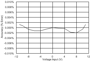
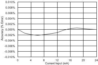
Figure 70 shows the measurement result accuracy for the ±10-V input application example. Figure 71 shows the measurement result accuracy for the 4-mA to 20-mA input application. The measurements were taken at TA = 25°C. Both application examples meet the required accuracy given in Table 28.
10.3 Dos and Don'ts
- Do partition the analog, digital, and power-supply circuitry into separate sections on the PCB.
- Do use a single ground plane for analog and digital grounds.
- Do place the analog components close to the ADC pins using short, direct connections.
- Do keep the SCLK pin free of glitches and noise.
- Do verify that the analog input voltages are within the specified absolute input-voltage range under all input conditions.
- Do tie unused input pins to proper voltage levels to minimize on-channel input leakage current.
- Do provide current limiting to the analog inputs to protect against overvoltage faults.
- Do use a low-dropout linear regulator (LDO) to reduce ripple voltage generated by switch-mode power supplies.
- Do not allow the analog and digital power-supply voltages to exceed the Absolute Maximum Ratings under any conditions, including during power-up and power-down.
Figure 72 shows the dos and don'ts of circuit connections for the ADS1257.
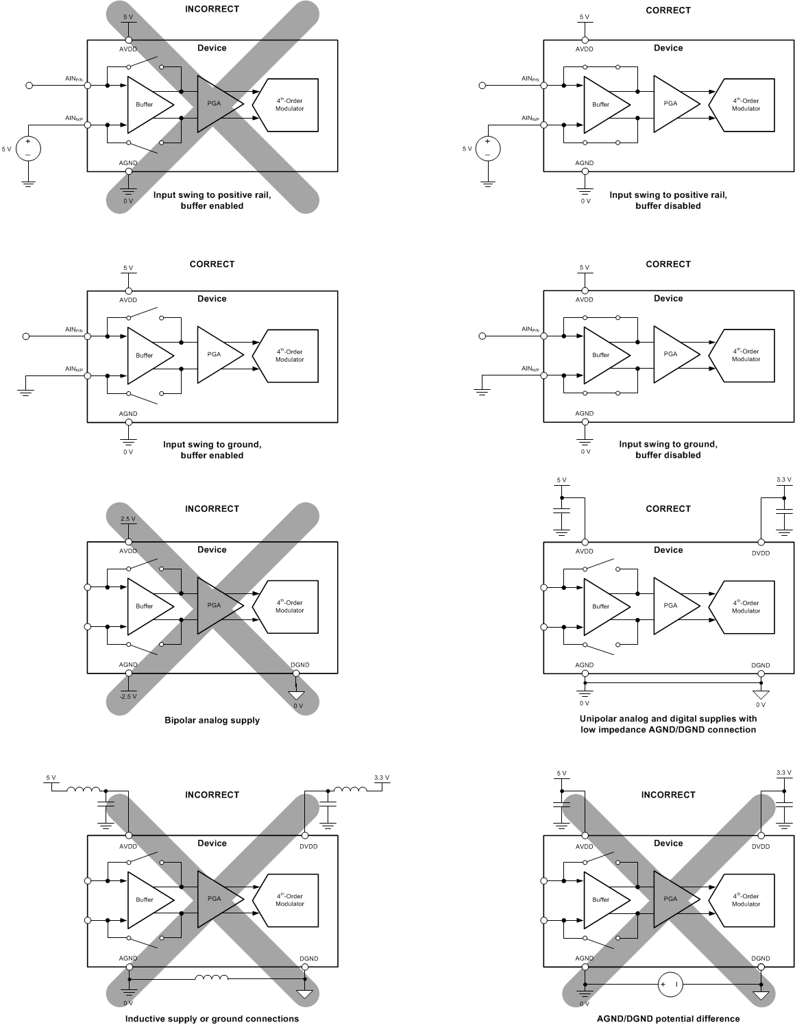 Figure 72. Do's and Don'ts Circuit Connections