SBAS533E March   2011  – February 2023 ADS4222 , ADS4225 , ADS4226 , ADS4242 , ADS4245 , ADS4246

PRODUCTION DATA  

  1. Features
  2. Applications
  3. Description
  4. Revision History
  5. Description (continued)
  6. Pin Configuration and Functions
    1.     Pin Functions – LVDS Mode
    2.     Pin Functions – CMOS Mode
  7. Specifications
    1. 7.1  Absolute Maximum Ratings
    2. 7.2  ESD Ratings
    3. 7.3  Recommended Operating Conditions
    4. 7.4  Thermal Information
    5. 7.5  Electrical Characteristics: ADS4246, ADS4245, ADS4242
    6. 7.6  Electrical Characteristics: ADS4226, ADS4225, ADS4222
    7. 7.7  Electrical Characteristics: General
    8. 7.8  Digital Characteristics
    9. 7.9  Timing Requirements: LVDS and CMOS Modes (1)
    10. 7.10 Serial Interface Timing Characteristics (1)
    11. 7.11 Reset Timing (Only When Serial Interface Is Used)
    12. 7.12 Typical Characteristics
      1. 7.12.1 ADS4246
      2. 7.12.2 ADS4245
      3. 7.12.3 ADS4242
      4. 7.12.4 ADS4226
      5. 7.12.5 ADS4225
      6. 7.12.6 ADS4222
      7. 7.12.7 General
      8. 7.12.8 Contour
  8. Detailed Description
    1. 8.1 Overview
    2. 8.2 Functional Block Diagrams
    3. 8.3 Feature Description
      1. 8.3.1 Analog Input
        1. 8.3.1.1 Drive Circuit Requirements
        2. 8.3.1.2 Driving Circuit
      2. 8.3.2 Clock Input
      3. 8.3.3 Digital Functions
      4. 8.3.4 Gain for SFDR/SNR Trade-off
      5. 8.3.5 Offset Correction
    4. 8.4 Device Functional Modes
      1. 8.4.1 Power-Down
        1. 8.4.1.1 Global Power-Down
        2. 8.4.1.2 Channel Standby
        3. 8.4.1.3 Input Clock Stop
    5. 8.5 Programming
      1. 8.5.1 47
      2. 8.5.2 Parallel Configuration Only
      3. 8.5.3 Serial Interface Configuration Only
      4. 8.5.4 Using Both Serial Interface and Parallel Controls
      5. 8.5.5 Parallel Configuration Details
      6. 8.5.6 Serial Interface Details
        1. 8.5.6.1 Register Initialization
        2. 8.5.6.2 Serial Register Readout
      7. 8.5.7 Digital Output Information
        1. 8.5.7.1 Output Interface
        2. 8.5.7.2 DDR LVDS Outputs
        3. 8.5.7.3 LVDS Buffer
        4. 8.5.7.4 Parallel CMOS Interface
        5. 8.5.7.5 CMOS Interface Power Dissipation
        6. 8.5.7.6 Multiplexed Mode of Operation
        7. 8.5.7.7 Output Data Format
    6. 8.6 Register Maps
      1. 8.6.1 64
      2. 8.6.2 Description Of Serial Registers
  9. Application and Implementation
    1. 9.1 Application Information
    2. 9.2 Typical Application
      1. 9.2.1 Design Requirements
      2. 9.2.2 Detailed Design Procedure
        1. 9.2.2.1 Analog Input
        2. 9.2.2.2 Clock Driver
        3. 9.2.2.3 Digital Interface
        4. 9.2.2.4 SNR and Clock Jitter
      3. 9.2.3 Application Curves
    3. 9.3 Power Supply Recommendations
      1. 9.3.1 Sharing DRVDD and AVDD Supplies
      2. 9.3.2 Using DC/DC Power Supplies
      3. 9.3.3 Power Supply Bypassing
    4. 9.4 Layout
      1. 9.4.1 Layout Guidelines
        1. 9.4.1.1 Grounding
        2. 9.4.1.2 Supply Decoupling
        3. 9.4.1.3 Exposed Pad
        4. 9.4.1.4 Routing Analog Inputs
      2. 9.4.2 Layout Example
  10. 10Device and Documentation Support
    1. 10.1 Device Support
      1. 10.1.1 Device Nomenclature
    2. 10.2 Documentation Support
      1. 10.2.1 Related Documentation
    3. 10.3 Support Resources
    4. 10.4 Trademarks
    5. 10.5 Electrostatic Discharge Caution
    6. 10.6 Glossary
  11. 11Mechanical, Packaging, and Orderable Information

Package Options

Mechanical Data (Package|Pins)
Thermal pad, mechanical data (Package|Pins)
Orderable Information

Multiplexed Mode of Operation

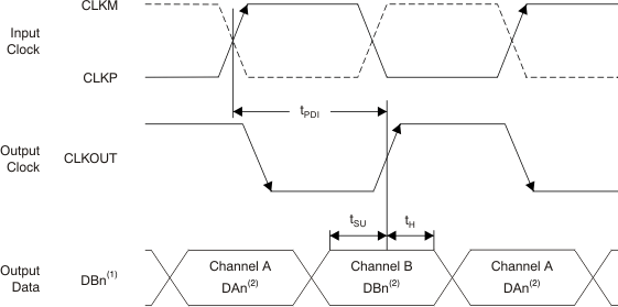
In this mode, the digital outputs of both channels are multiplexed and output on a single bus (DB[13:0] pins), as shown in #SBAS509IMG3393. The channel A output pins (DA[13:0]) are in 3-state. Because the output data rate on the DB bus is effectively doubled, this mode is recommended only for low sampling frequencies (less than 80MSPS). This mode can be enabled using the POWER-DOWN MODE register bits or using the CTRL[3:1] parallel pins.
GUID-7A1D6864-A9E1-47B6-879C-D888A200BA94-low.gif
In multiplexed mode, both channels outputs come on the channel B output pins.
Dn = bits D0, D1, D2, etc.
Figure 8-25 Multiplexed Mode Timing Diagram