SBAS931B January   2019  – July 2022 ADS8353-Q1

PRODUCTION DATA  

  1. 1Features
  2. 2Applications
  3. 3Description
  4. 4Revision History
  5. 5Pin Configuration and Functions
  6. 6Specifications
    1. 6.1 Absolute Maximum Ratings
    2. 6.2 ESD Ratings
    3. 6.3 Thermal Information
    4. 6.4 Recommended Operating Conditions
    5. 6.5 Electrical Characteristics
    6. 6.6 Timing Requirements
    7. 6.7 Switching Characteristics
    8. 6.8 Timing Diagram
    9. 6.9 Typical Characteristics
  7. 7Detailed Description
    1. 7.1 Overview
    2. 7.2 Functional Block Diagram
    3. 7.3 Feature Description
      1. 7.3.1 Reference
      2. 7.3.2 Analog Inputs
        1. 7.3.2.1 Analog Input: Full-Scale Range Selection
        2. 7.3.2.2 Analog Input: Single-Ended and Pseudo-Differential Configurations
      3. 7.3.3 Transfer Function
    4. 7.4 Device Functional Modes
    5. 7.5 Programming
      1. 7.5.1 Serial Interface
      2. 7.5.2 Write to User-Programmable Registers
      3. 7.5.3 Data Read Operation
        1. 7.5.3.1 Reading User-Programmable Registers
        2. 7.5.3.2 Conversion Data Read
          1. 7.5.3.2.1 32-CLK, Dual-SDO Mode (CFR.B11 = 0, CFR.B10 = 0, Default)
          2. 7.5.3.2.2 32-CLK, Single-SDO Mode (CFR.B11 = 0, CFR.B10 = 1)
      4. 7.5.4 Low-Power Modes
        1. 7.5.4.1 STANDBY Mode
        2. 7.5.4.2 Software Power-Down (SPD) Mode
      5. 7.5.5 Frame Abort, Reconversion, or Short-Cycling
    6. 7.6 Register Maps
      1. 7.6.1 ADS8353-Q1 Registers
  8. 8Application and Implementation
    1. 8.1 Application Information
      1. 8.1.1 Input Amplifier Selection
      2. 8.1.2 Charge Kickback Filter
    2. 8.2 Typical Application
      1. 8.2.1 Design Requirements
      2. 8.2.2 Detailed Design Procedure
      3. 8.2.3 Application Curve
    3. 8.3 Power Supply Recommendations
    4. 8.4 Layout
      1. 8.4.1 Layout Guidelines
      2. 8.4.2 Layout Example
  9. 9Device and Documentation Support
    1. 9.1 Device Support
      1. 9.1.1 Development Support
    2. 9.2 Documentation Support
      1. 9.2.1 Related Documentation
    3. 9.3 Receiving Notification of Documentation Updates
    4. 9.4 Support Resources
    5. 9.5 Trademarks
    6. 9.6 Electrostatic Discharge Caution
    7. 9.7 Glossary
      1.      Mechanical, Packaging, and Orderable Information

Package Options

Mechanical Data (Package|Pins)
Thermal pad, mechanical data (Package|Pins)
Orderable Information

Software Power-Down (SPD) Mode

In software power-down (SPD) mode, all internal circuits (including the internal references) are powered down. However, the contents of the REFDAC_A and REFDAC_B registers are retained.

As shown in Figure 7-10, to enter SPD mode, the device must be selected (by bringing CS low) and SDI must be kept high for a minimum of 48 SCLK cycles during frame (F). The device goes to SPD on the CS rising edge following frame (F). While in SPD mode, SDO_A and SDO_B go to 3-state irrespective of the status of the CS signal.

To remain in SPD mode, SDI must remain high in all subsequent frames.
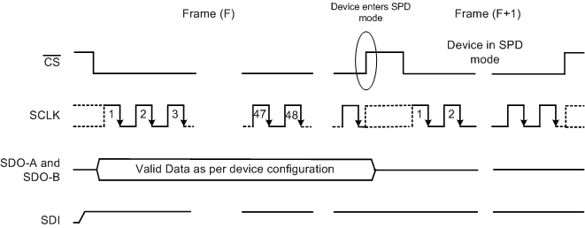
GUID-9B323D70-D265-4965-8E1A-4287188985A2-low.gifFigure 7-10 Enter SPD Mode

As shown in Figure 7-11, to exit SPD mode, the device must be selected (by bringing CS low) and SDI must be kept low for a minimum of 48 SCLK cycles during frame (F+3). The device starts powering-up on a CS rising edge following frame (F+3). After frame (F+3), a delay of tPU_SPD must elapse before programming the configuration register.

A valid write operation in frame (F+4) sets the device configuration for frame (F+5). Frame (F+4) must have at least 48 SCLK falling edges. Discard the output data in frame (F+4).

GUID-65282C90-1EB3-4F54-9F98-224AD0C890F6-low.gif
N is a function of the device configuration, as described in Table 7-4.
Figure 7-11 Exit SPD Mode

See the Section 6.6 table for timing specifications for this operating mode.